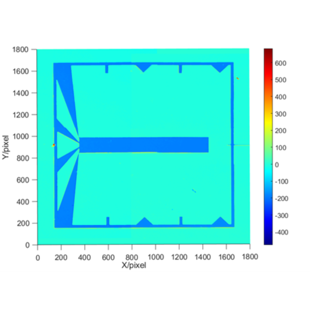
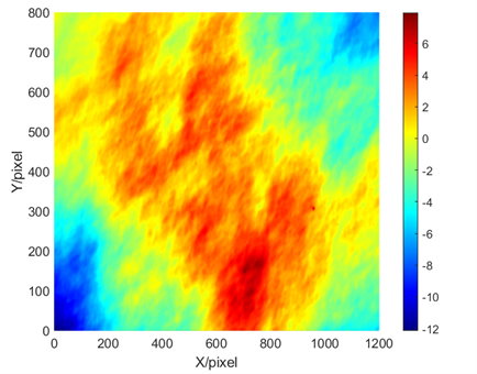
Image Gallery
Image Gallery
Knowledge Center
Image Gallery

Current Location:Home > Knowledge Center > Image Gallery

Filter by:
-Holes Array

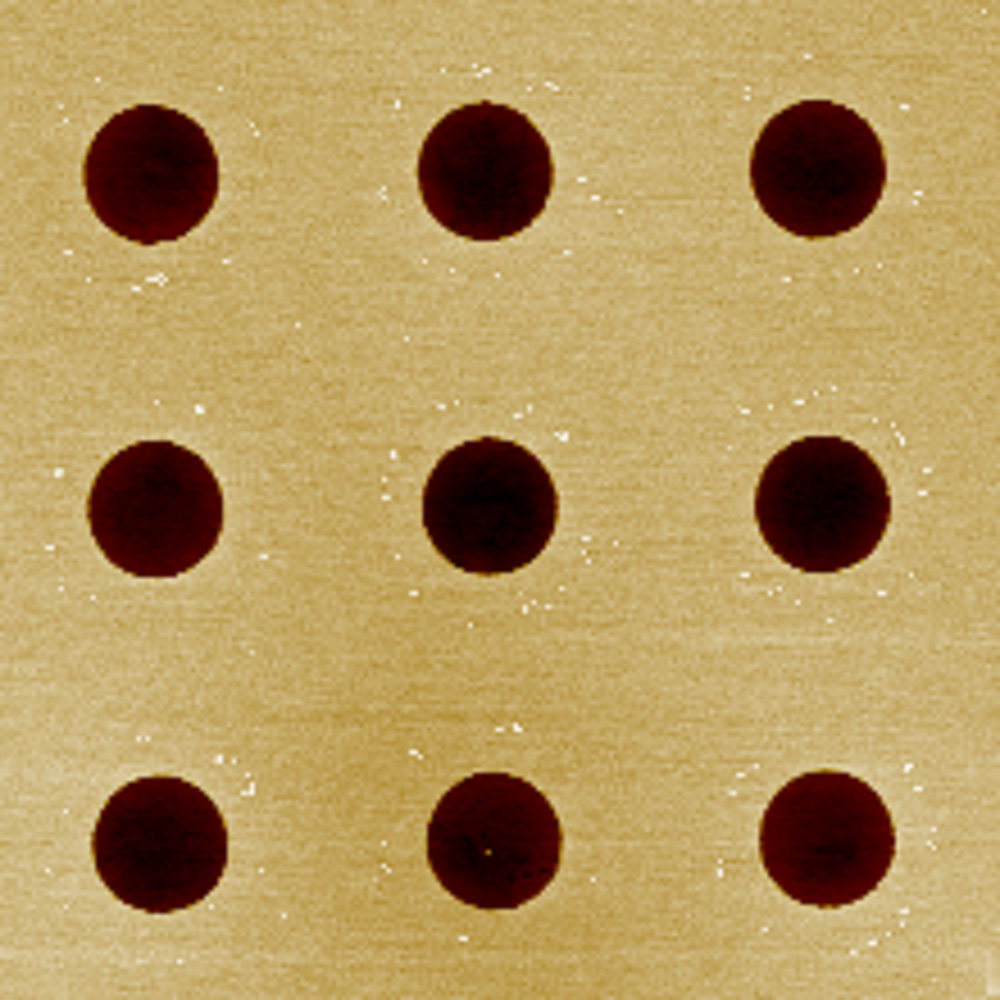
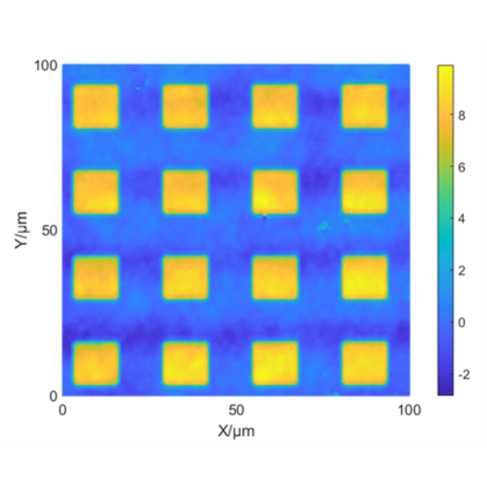
This is an image of a micro-holes array with a scanning range of 30 μm after the Chemical Mechanical Polishing (CMP) process. The CMP process is a key technique for wafer flattening. It can provide a strong guarantee for the improvement of the CMP process in terms of surface roughness and surface shape measurement.

">
CMP Micro-Holes Array
  • SiC Surface
    SiC Surface
  • The Surface Potential of SRAM
    The Surface Potential of SRAM
  • Standard Wafer
    Standard Wafer
  • Microelectrode
    Microelectrode
  • 182 nm Standard Step Height
    182 nm Standard Step Height
  • Girds Matrix
    Girds Matrix
  • Polished Silicon Wafer
    Polished Silicon Wafer