Home
Home
Products
Products
Atomic Force Microscope (AFM)
AFM-Baritone
AFM-Piccolo
AFM-Tuba
AFM-Tenor
AFM-Tuner
White Light Interferometry (WLI)
WLI-Marimba
Integrated Systems
AFM-WLI Duet
Accessories
AFM Probes
Applications
Applications
Semiconductor
Display
2D Materials
Thin Film
Knowledge Center
Knowledge Center
Image Gallery
Case Studies
Webinars
FreeSpirit Academy
Download Center
News & Events
News & Events
News
Events
Company
Company
Overview
Careers
Social Media
Contact
Contact
Contact Information
Online Enquiries
EN
EN
中
×
Knowledge Center
Image Gallery
Current Location:
Home
>
Knowledge Center
>
Image Gallery
Filter by:
System
All
AFM-Piccolo
AFM-Baritone
AFM-Tenor
AFM-Tuba
AFM-Tuner
WLI-Marimba
AFM-WLI Duet
Application
All
Semiconductor
Display
2D Materials
Thin films
Polymer
MEMS
Metals
Optical Element
Metal
ss="dropC">
All
AFM-Piccolo
AFM-Baritone
AFM-Tenor
AFM-Tuba
AFM-Tuner
WLI-Marimba
AFM-WLI Duet
Application
All
Semiconductor
Display
2D Materials
Thin films
Polymer
MEMS
Metals
Optical Element
Metal
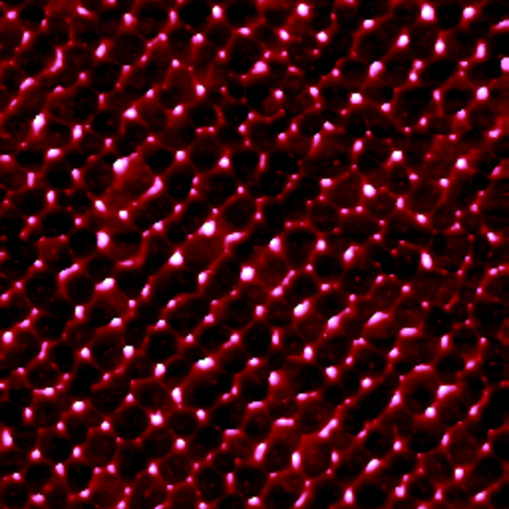
5 μm. The roughness of the whole image is approximately 10 nm, and the grain size is about 150 nm. LTPS is the abbreviation of Low Temperature Poly-Silicon, and it is mainly used in the display industry and solar photovoltaic industry.">
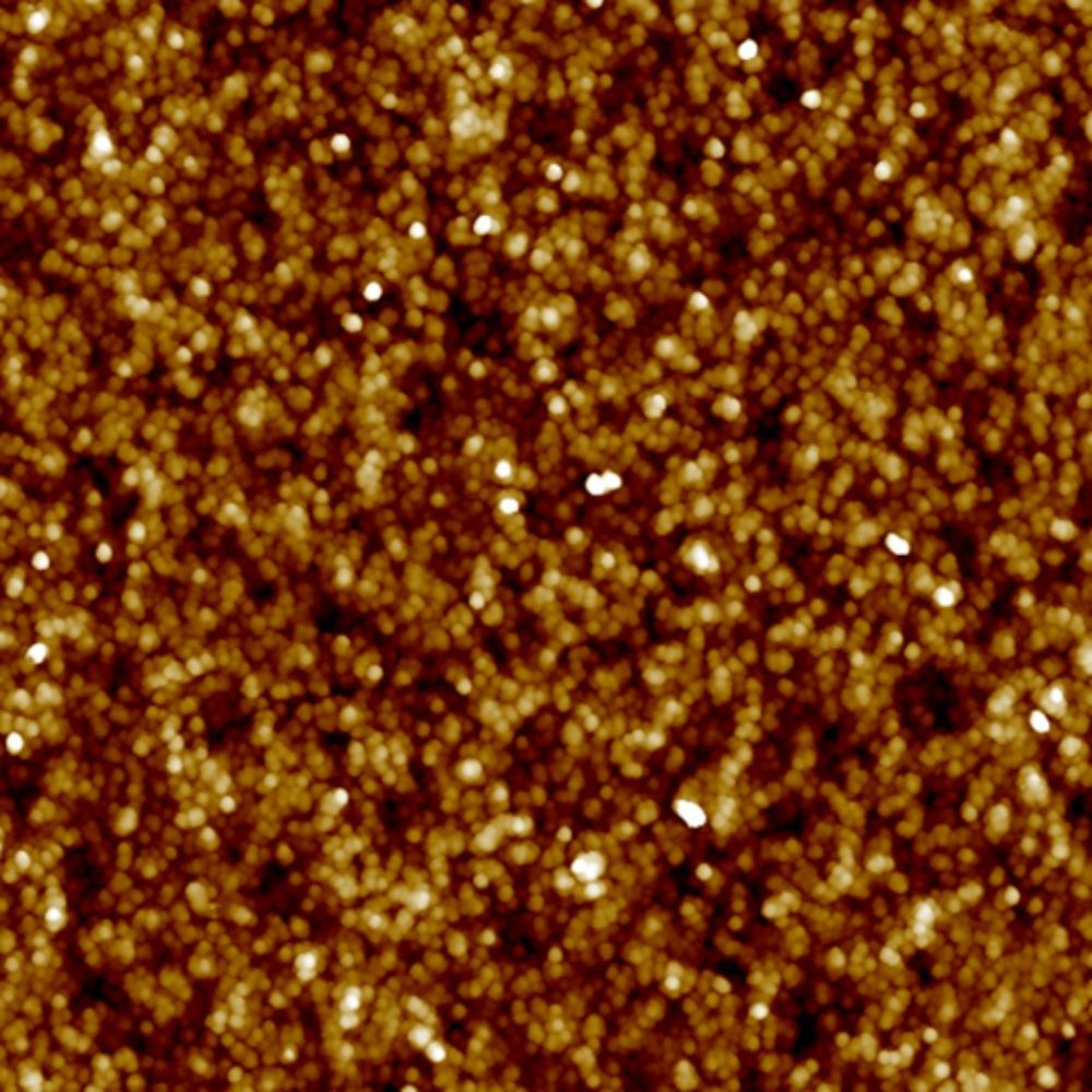
LTPS Grain
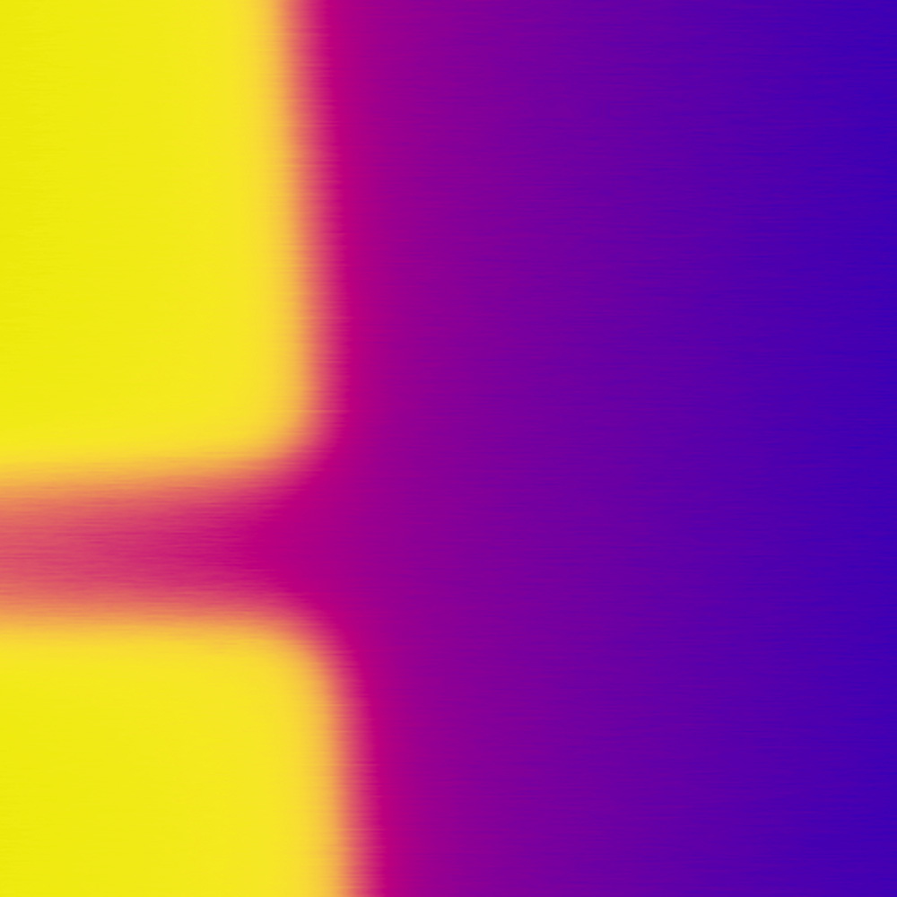
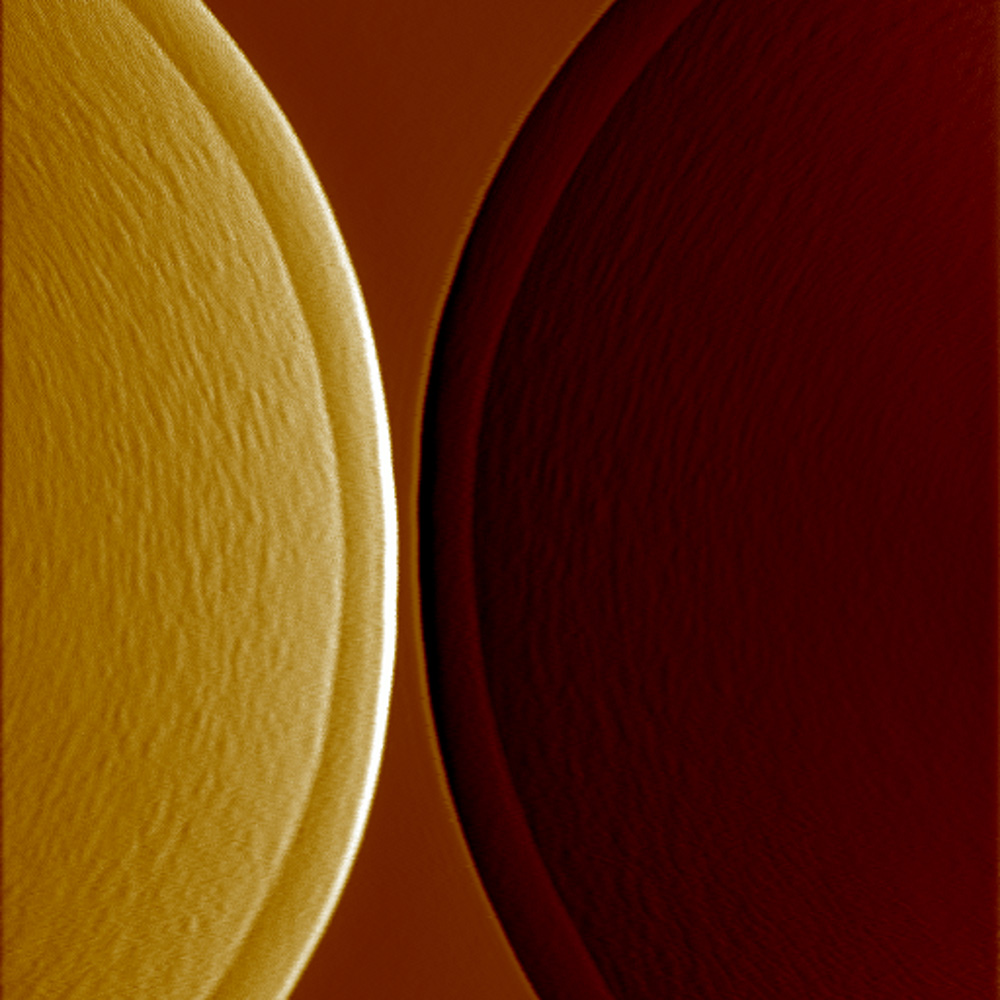
The Surface Potential of Au-Al Material
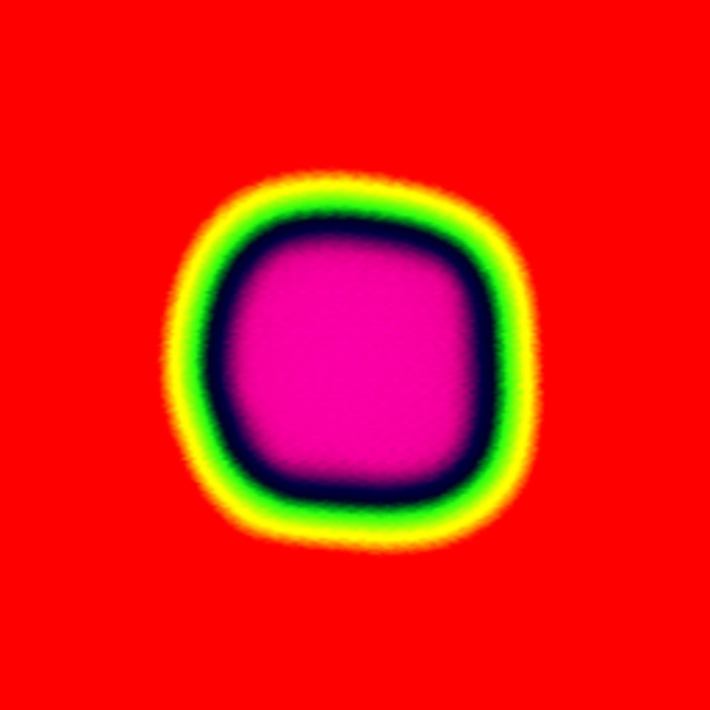
Patterned Sapphire Substrate (PSS)
OLED Pattern
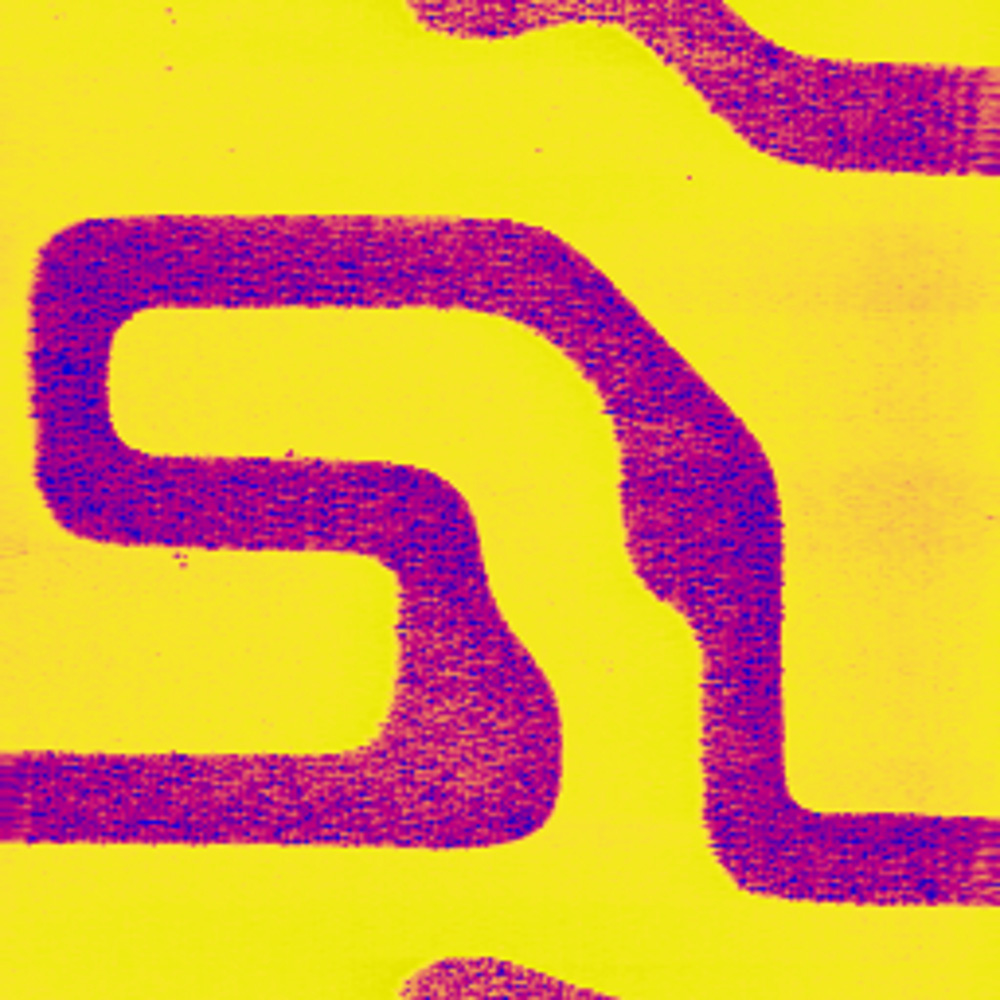
ETL Structure
The Edge Structure of PSS
Glass Substrate