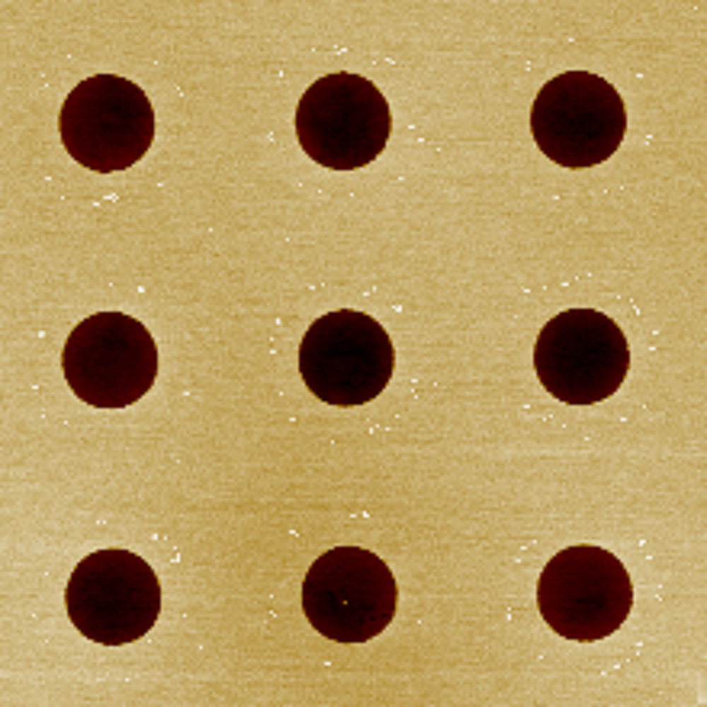
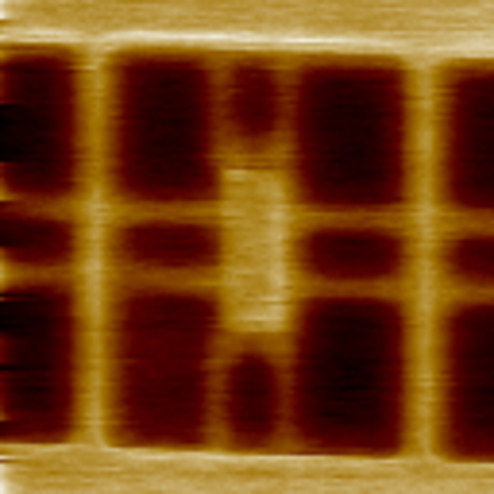
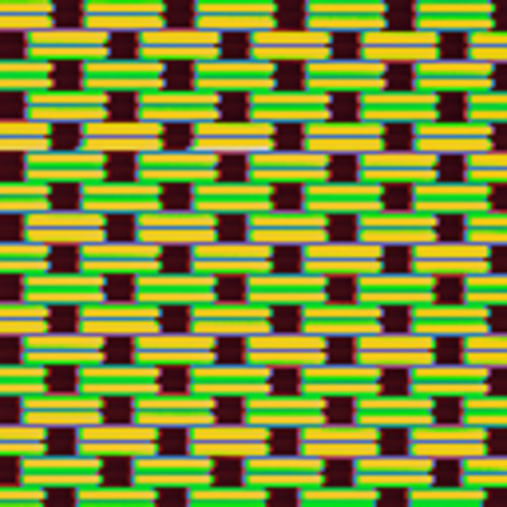
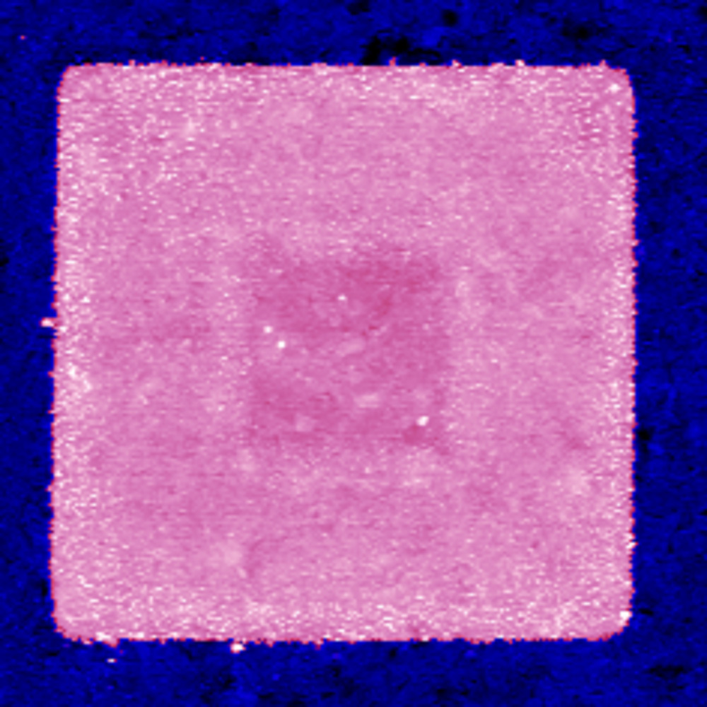
This is a surface topography image of a standard wafer with a scanning range of 20 μm. The image can be used to determine whether the periodic structure of the wafer processing conforms to expectations, and provide a reference for identifying processing defects.