Knowledge Center
Case Studies


AFM-WLI Duet is a coaxial integrated system of the FreeSpirit ultra-thin head AFM-Piccolo and the Linnik type WLI-Marimba. The design of the AFM-Piccolo head is unique. Its effective thickness is less than 8 mm, and the thickness of the base part is less than 10 cm, making it highly convenient for integration with other system, including the White Light Interferometer (WLI). The Linnik type design of WLI-Marimba enables a sufficient working distance for the WLI, perfectly matching the desktop sized ultra-thin AFM-Piccolo head.

In certain applications where users require both large-scale rapid measurements and small-scale high-resolution measurements, the AFM-WLI Duet provides a convenient cross-scale measurement solution. It utilizes WLI for large-scale rapid measurements and AFM for small-area high-resolution measurements. The combination of both offers users a convenient in-situ cross-scale topography characterization solution.
The following shows a test case utilizing the combination of FreeSpirit AFM and WLI.
Figure 1 shows test results of a square grid using the AFM-WLI Duet. The Visual Image is directly observed with an optical microscope, revealing the square grid and probe cantilever. The central square region is selected for WLI imaging, as shown in the blue-green image with a 550 μm field of view. The red section image represents the height difference cross-section of the square grid. The protruding region of square grid is selected for AFM imaging, as shown in the yellow-brown image with a 50 μm scan range. The blue section image represents the grid height difference cross-section with a step height of approximately 105 nm. This data is consistent with measurements from the WLI.
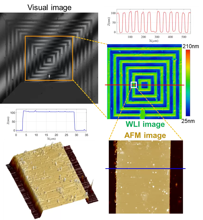
Figure 1 Square Grid Image
Figure 2 shows images obtained by testing static random-access memory (SRAM) using the AFM-WLI Duet. The blue image on the left represents the WLI image of the SRAM with a field of view of 500 μm. The red part in the image is the AFM probe cantilever. The right side displays the topography image of the AFM test with a scan range of 20 μm. During testing, a large-scale WLI imaging of the SRAM is first obtained. Then select the interest regions and use the AFM probe to scan the small-scale area.
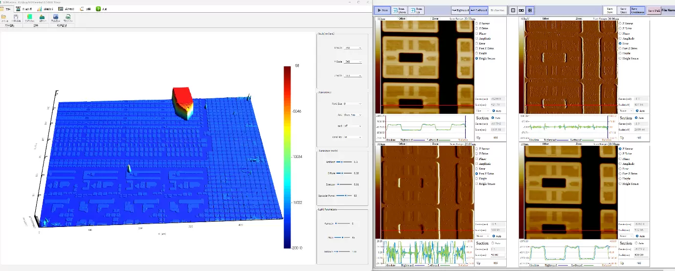
Figure 2 SRAM Image

SiC is a wide-bandgap semiconductor material. Due to its superior physical and electrical properties, it plays an increasingly vital role in the modern semiconductor industry, particularly in electronic devices operating under extreme conditions such as high voltage, high frequency, high temperature, and high power. Simultaneously, since parameters such as surface topography, crystal quality, and roughness significantly impact the performance of SiC materials and devices, AFM serves as an indispensable nanoscale surface analysis tool in SiC-related research and production.
Although SiC has outstanding electrical and thermal properties, numerous challenges persist in material preparation, crystal growth, surface treatment, and device fabrication—including surface roughness control, epitaxial layer quality, and crystal defects, etc. Therefore, to fully leverage exceptional performance of SiC, strict control over material quality, surface condition, and processing precision is essential. As a high-resolution, non-destructive surface measurement and analysis tool, AFM has become an indispensable instrument in SiC material and device R&D, production, and quality control. Through precise AFM characterization, researchers and engineers gain deep insights into the microscopic world of SiC surfaces and interfaces, continuously advancing SiC semiconductor technology toward higher performance and reliability.
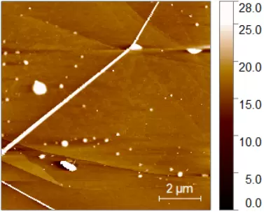
As shown in the figure below, this is the scanning result of FreeSpirit AFM. It shows a 500 nm scan range of SiC atomic steps, with a step height of approximately 0.75 nm.
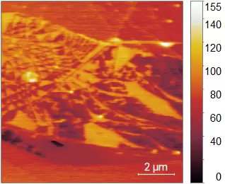
As shown in the figure below, this is an image obtained by scanning the SiC surface using a FreeSpirit AFM. The scanning range is 10 μm, and the roughness of the C-surface is 0.72 nm.
Low temperature polycrystalline silicon (LTPS) is a technology used to manufacture thin film transistors (TFT). It is widely applied in the modern display panel industry, particularly in high-end small-to-medium-sized display devices such as smartphones, tablet computers, automotive displays, premium laptops, and emerging flexible displays and AMOLED screens.
AFM plays an indispensable role in both the research and production testing of LTPS technology. This is mainly because the core of LTPS lies in the microscopic characteristics of its polycrystalline silicon thin film, including surface topography, grain structure, crystalline quality, and electrical property distribution. These characteristics directly affect the performance of TFT devices, such as mobility, threshold voltage, uniformity, and reliability. Uniform grain size enhances electron mobility; surface roughness affects the uniformity and interface quality of subsequent processes such as gate insulation layer and source/drain formation; defective grain boundaries impair carrier transport and device consistency; crystalline defects and voids reduce the electrical stability and lifetime of TFT.
As an ultra-high-resolution, non-destructive tool for analyzing surface topography and material properties, AFM enables nanoscale or even atomic-level characterization of nanoscale features such as surface roughness, grain size and distribution, grain boundary density and orientation, crystalline defects, and voids. It provides key data support for process optimization, defect analysis, mechanism research, and yield improvement in the modern display panel industry, particularly for LTPS applications.
The following two AFM scan images of LTPS demonstrate the measurement capabilities of the FreeSpirit AFM. The two images below show LTPS grains with slightly different crystal orientations, both scanned over a 5 μm area. Both images show a roughness of approximately 10 nm, uniform grain distribution without obvious defects, and grain sizes around 150 nm.
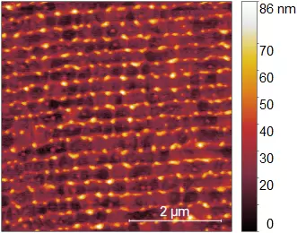
LTPS Surface Crystalline Grain Orientation Image
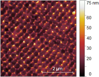
LTPS Surface Crystalline Grain Orientation Image
As one of the major breakthroughs in 21st-century materials science, 2D materials demonstrate revolutionary application potential across electronics, energy, sensing, optoelectronics, medicine, and environmental fields due to their unique structures and exceptional properties. Despite facing challenges in preparation, stability, integration, and other aspects, with the continuous advancement of technology and in-depth research, 2D materials are expected to drive technological innovation in multiple industries in the coming decades, becoming the core foundational material for building the next generation of intelligent, flexible, and efficient devices.
Graphene, transition metal dichalcogenides (e.g., MoS₂), black phosphorus (BP), hexagonal boron nitride (h-BN), MXene, and 2D transition metal carbides/nitrides are all representative examples of 2D materials. With its high spatial resolution, multimodal measurement capabilities, low sample damage, and adaptability across diverse environments, AFM plays a central role in fundamental research, performance characterization, and device application exploration of 2D materials. It remains one of the most critical characterization tools, particularly for thickness measurement, surface topography, nanomechanical and nanoelectrical property analysis, and heterostructure investigation.
The following shows typical results obtained using the FreeSpirit AFM to test 2D materials, with h-BN serving as an example. As shown in the following figures, these are topographical and surface potential images of hexagonal boron nitride (h-BN) with a scanning range of 10 μm. Analysis of the topographical image reveals that the thickness of this h-BN monolayer is approximately 0.3 nm, with a surface roughness of about 0.4 nm in the flat regions. The surface potential image clearly shows the irregular distribution of surface potential within the specially treated h-BN. Analysis of h-BN thickness, surface roughness, and surface potential provides intuitive data support for understanding the effects of layer number on electronic and lattice structures, as well as local work function variations induced by doping effects.
h-BN Surface Topography Image (Vertical Coordinates Unit: nm)
h-BN Surface Potential Image (Vertical Coordinates Unit: mV)

留言提交中... |