Knowledge Center
Image Gallery


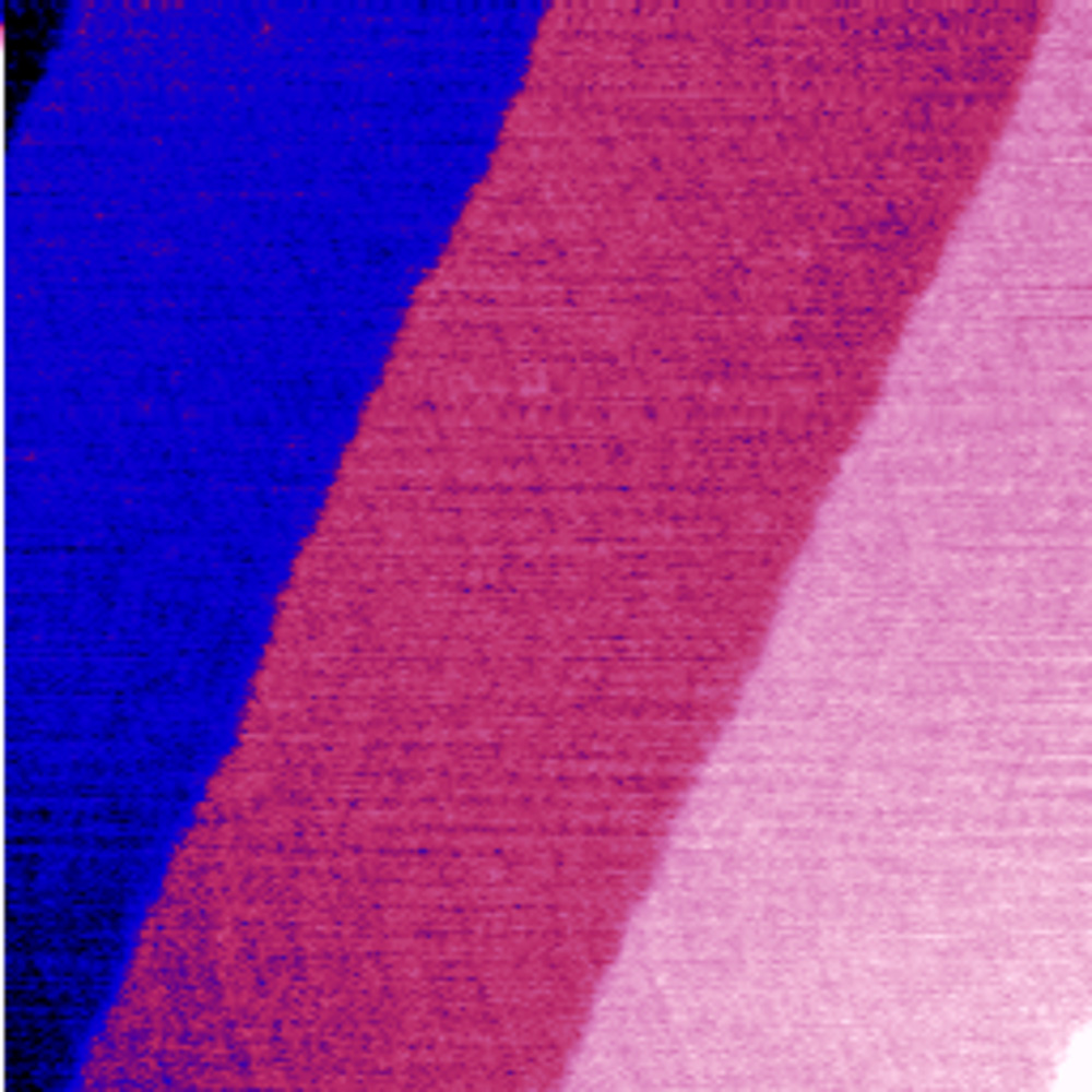
This is an image of SiC atomic step with a scanning range of 500 nm, and the step height is approximately 0.75 nm. SiC, as a representative material of wide bandgap semiconductors, is regarded as an ideal material for manufacturing high-power semiconductor devices.
">
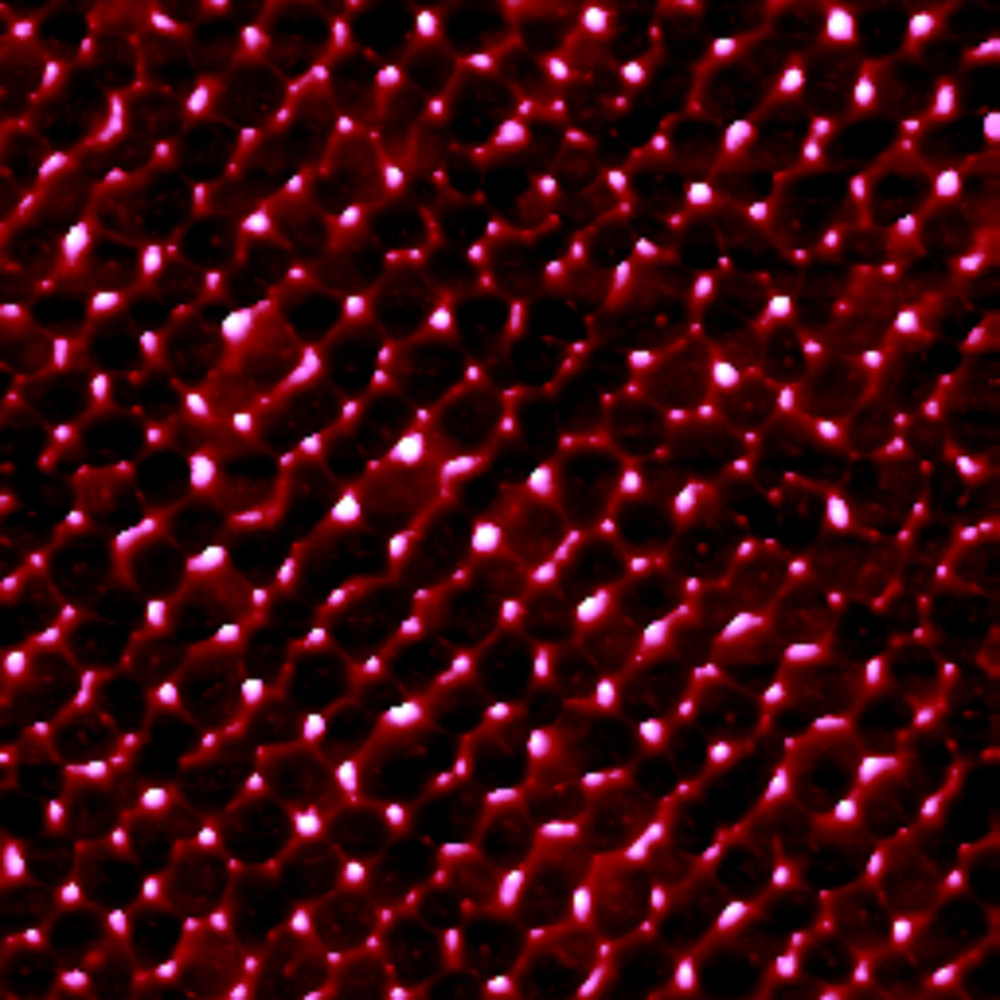
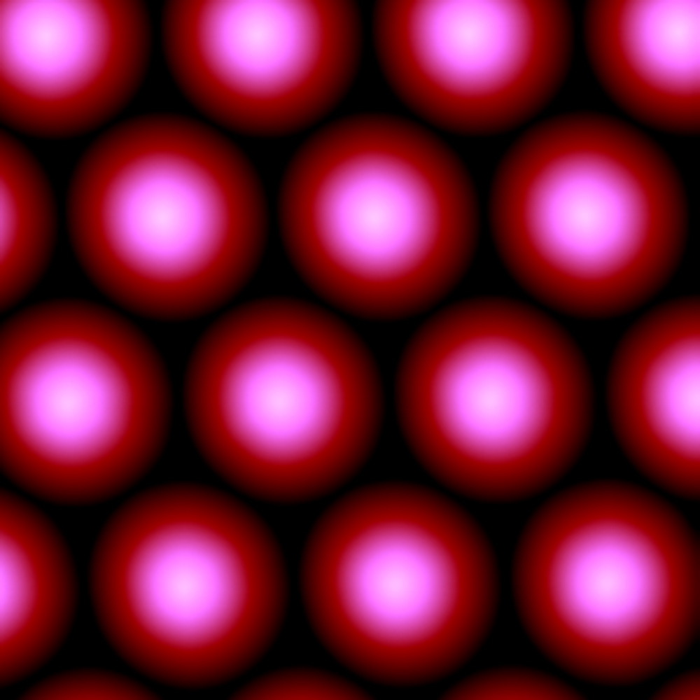 The height of PSS is about 2 μm and the bottom width is about 3 μm. Sapphire wafers are the most widely used substrate material in the semiconductor lighting industry, and using PSS is a common method to improve the luminous efficiency of semiconductor lighting devices.">