Image Gallery
Image Gallery
Knowledge Center
Image Gallery

Current Location:Home > Knowledge Center > Image Gallery

Filter by:
ads/upload/20251030/25103014223ON.jpg" data-sub-html="

Patterned Sapphire Substrate (PSS)

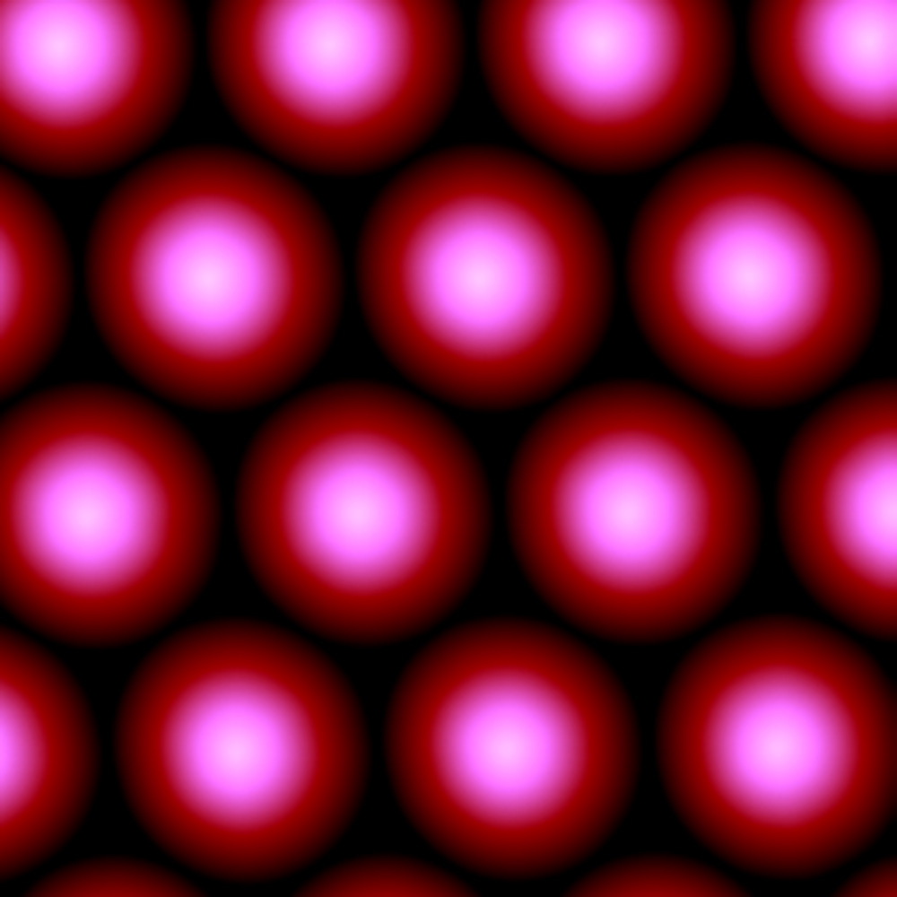
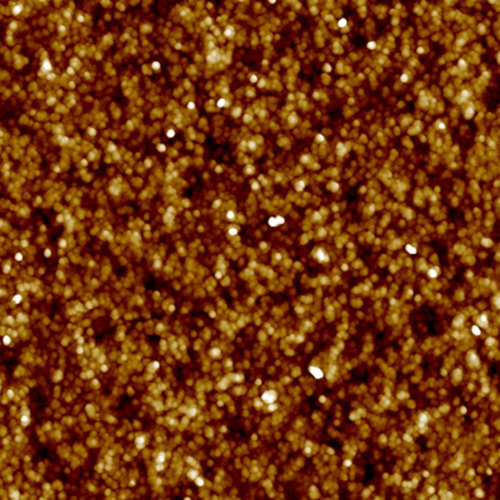
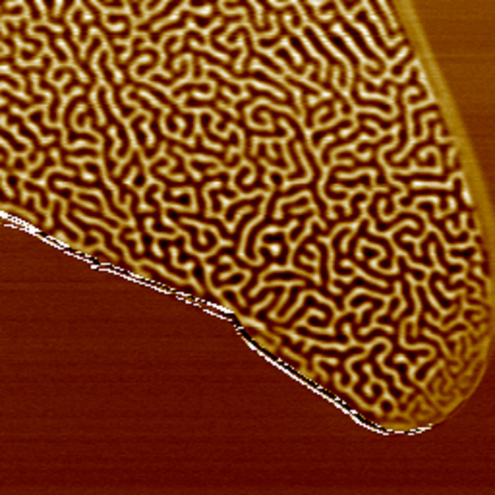
This is an image of a PSS with a scanning range of 10 μm. The height of PSS is about 2 μm and the bottom width is about 3 μm. Sapphire wafers are the most widely used substrate material in the semiconductor lighting industry, and using PSS is a common method to improve the luminous efficiency of semiconductor lighting devices.

">
Patterned Sapphire Substrate (PSS)
  • OLED Pattern
    OLED Pattern
  • ETL Structure
    ETL Structure
  • The Edge Structure of PSS
    The Edge Structure of PSS
  • Glass Substrate
    Glass Substrate