Knowledge Center
Image Gallery

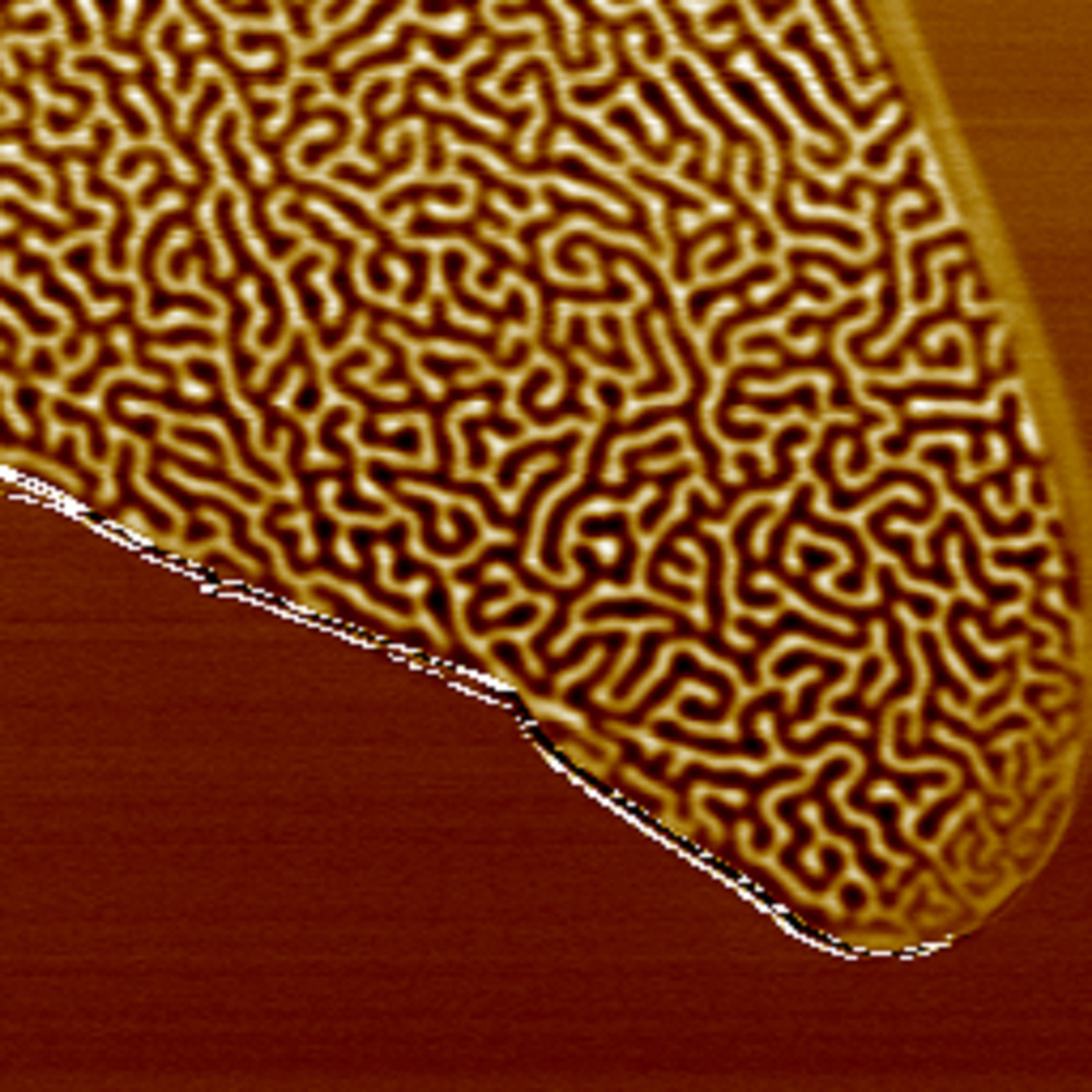
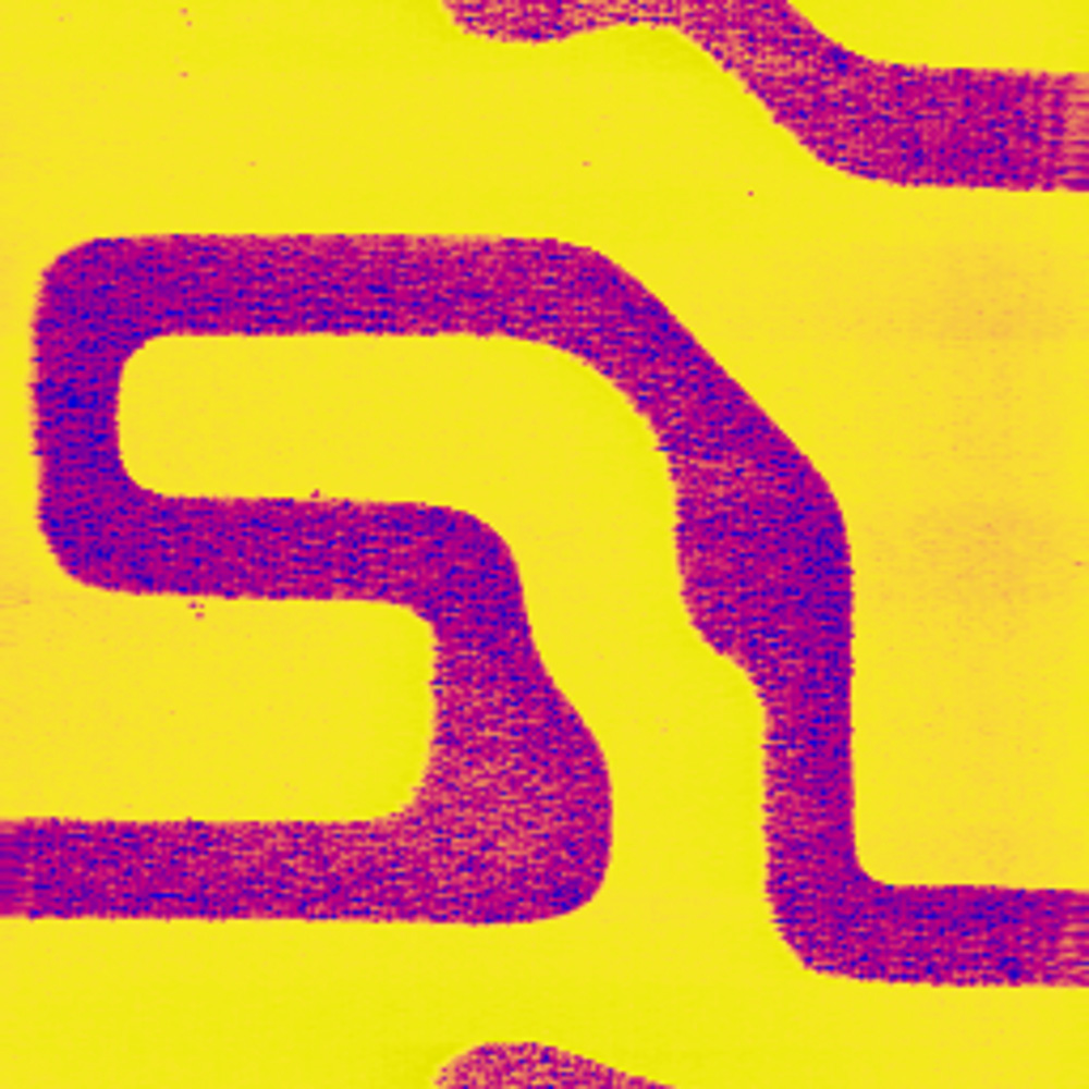
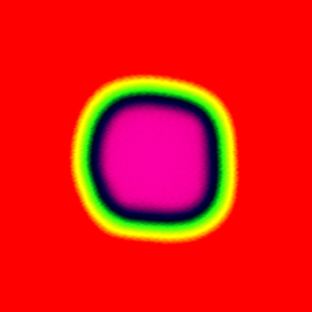
This is an image of a PSS with a scanning range of 10 μm. The height of PSS is about 2 μm and the bottom width is about 3 μm. Sapphire wafers are the most widely used substrate material in the semiconductor lighting industry, and using PSS is a common method to improve the luminous efficiency of semiconductor lighting devices.
">
Copyright © 2025 FreeSpirit (Shanghai) Precision Instrument Co., Ltd Shanghai ICP No. 2025145947-1 Privacy Policy Sitemap
Room 2109, 21st Floor, Building 2, Ruihong Enterprise World, 118 Feihong Road, Hongkou District, Shanghai


Copyright © 2025 FreeSpirit (Shanghai) Precision Instrument Co., Ltd Shanghai ICP No. 2025145947-1 Privacy Policy Sitemap