Knowledge Center
Image Gallery


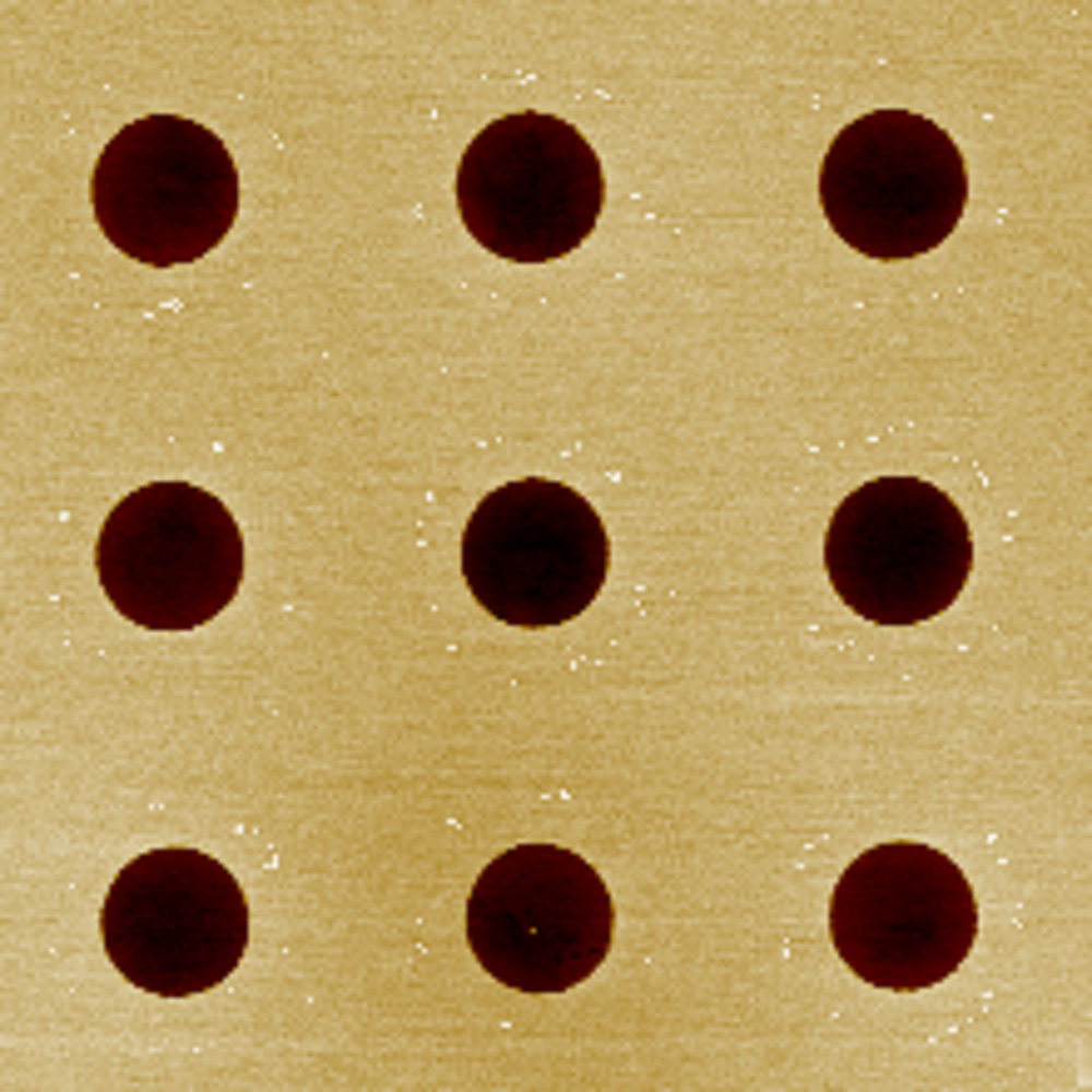
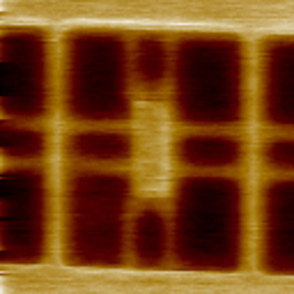
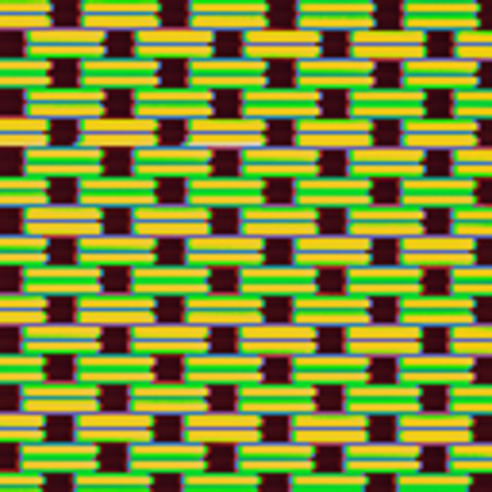
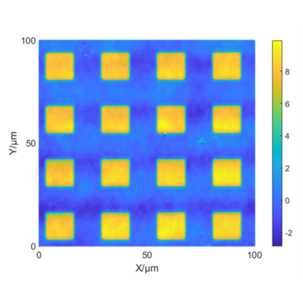
This is a surface topography image of a standard wafer with a scanning range of 20 μm. The image can be used to determine whether the periodic structure of the wafer processing conforms to expectations, and provide a reference for identifying processing defects.
">
Copyright © 2025 FreeSpirit (Shanghai) Precision Instrument Co., Ltd Shanghai ICP No. 2025145947-1 Privacy Policy Sitemap

留言提交中... |