Image Gallery
Image Gallery
Knowledge Center
Image Gallery

Current Location:Home > Knowledge Center > Image Gallery

  • SiC Atomic Step
    SiC Atomic Step
  • Patterned Sapphire Substrate (PSS)
    Patterned Sapphire Substrate (PSS)
  • CMP Micro-Holes Array
    CMP Micro-Holes Array
  • OLED Pattern
    OLED Pattern
  • ETL Structure
    ETL Structure
  • PLZT
    PLZT
  • SiC Surface
    SiC Surface
  • The Edge Structure of PSS
    The Edge Structure of PSS
  • The Surface Potential of SRAM 
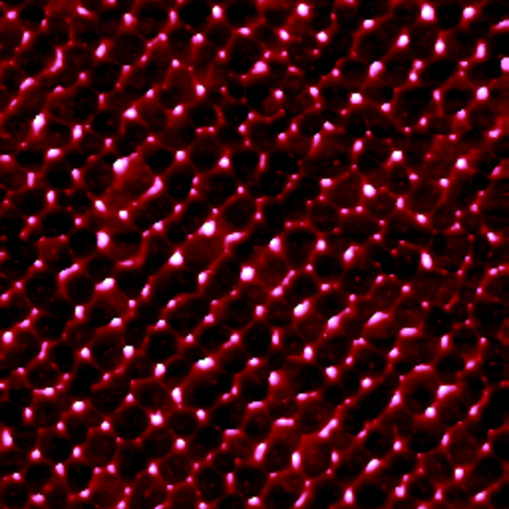
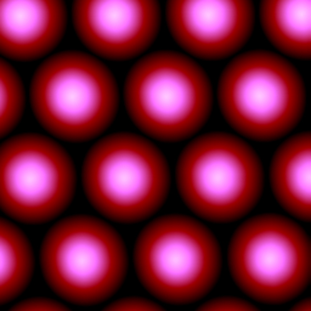
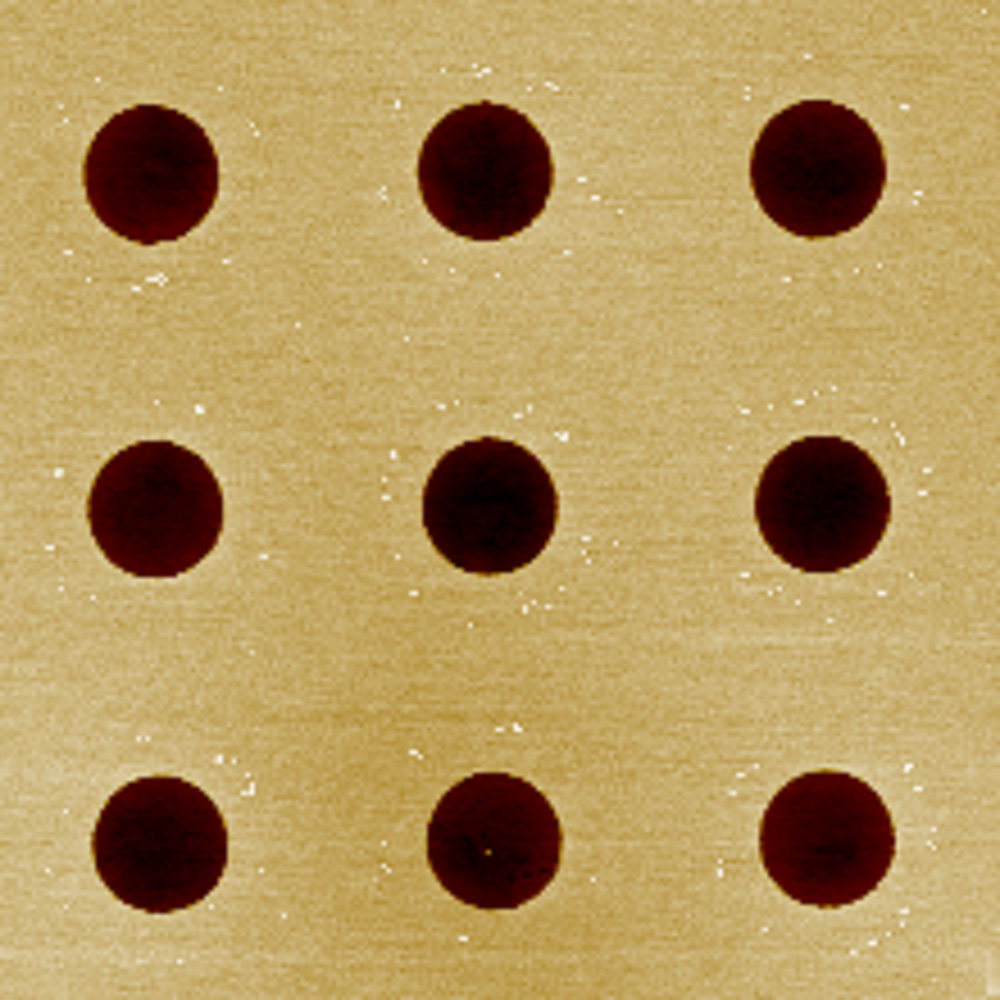
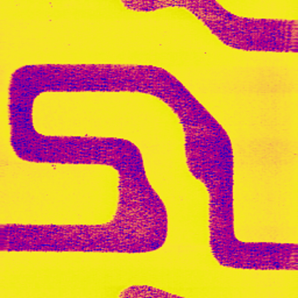
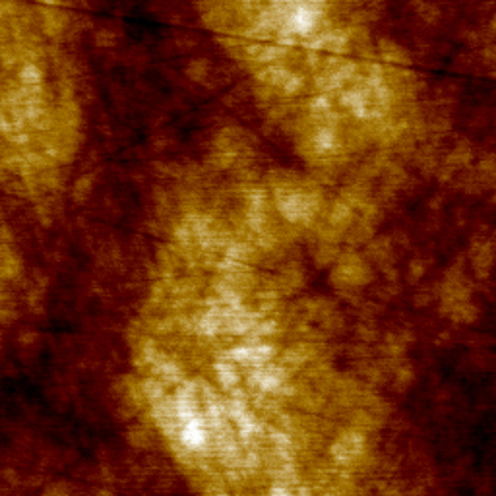
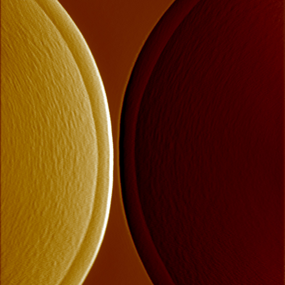
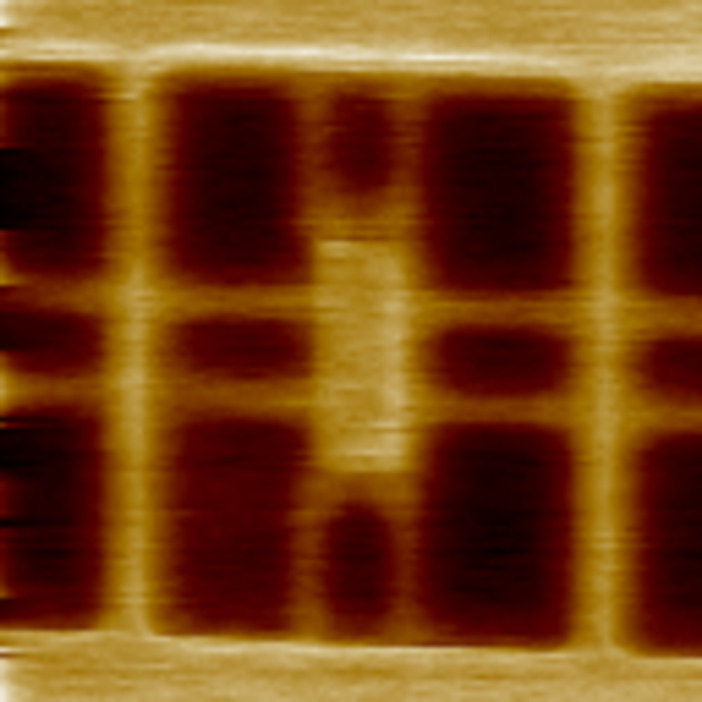
hether the periodic structure of the wafer processing conforms to expectations, and provide a reference for identifying processing defects.

    ">
    Standard Wafer
    Standard Wafer
  • Microelectrode
    Microelectrode
  • Polymer Particle
    Polymer Particle
  • Glass Substrate
    Glass Substrate