-
 LTPS Grain
 -
 The Surface Potential of Au-Al Material
 -
data-src="/uploads/upload/20251030/25103014230S28.jpg" data-sub-html="
CMP Micro-Holes Array
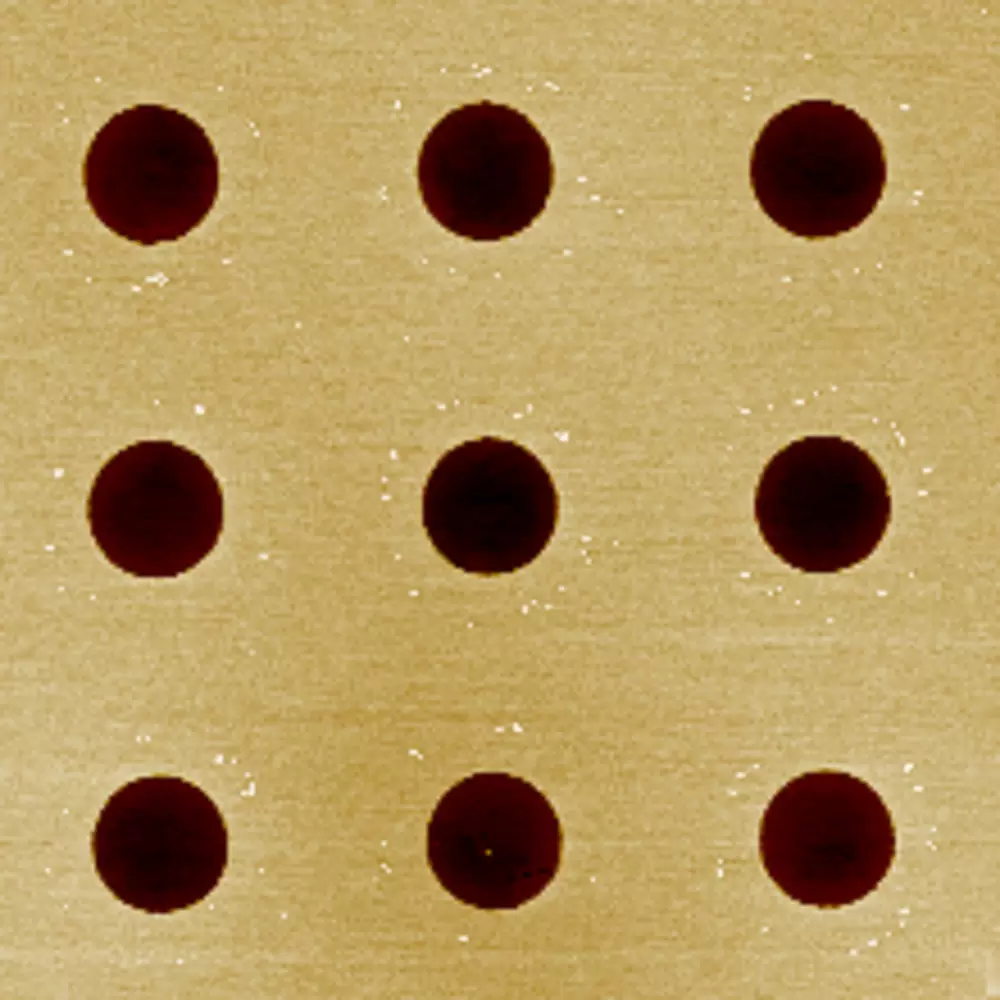
This is an image of a micro-holes array with a scanning range of 30 μm after the Chemical Mechanical Polishing (CMP) process. The CMP process is a key technique for wafer flattening. It can provide a strong guarantee for the improvement of the CMP process in terms of surface roughness and surface shape measurement.
"> CMP Micro-Holes Array
 -
 -Holes Array
This is an image of a micro-holes array with a scanning range of 30 μm after the Chemical Mechanical Polishing (CMP) process. The CMP process is a key technique for wafer flattening. It can provide a strong guarantee for the improvement of the CMP process in terms of surface roughness and surface shape measurement.
"> CMP Micro-Holes Array
 OLED Pattern
- Microelectrode
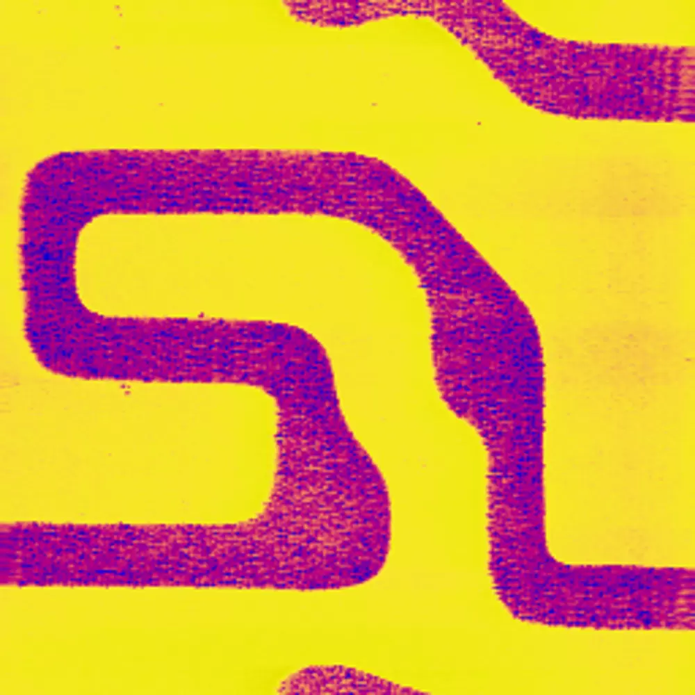
This is a microelectrode surface topography image with a scanning range of 28 μm, and its height is approximately 120 nm.
">Microelectrode -
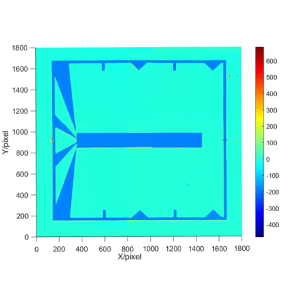 182 nm Standard Step Height
 -
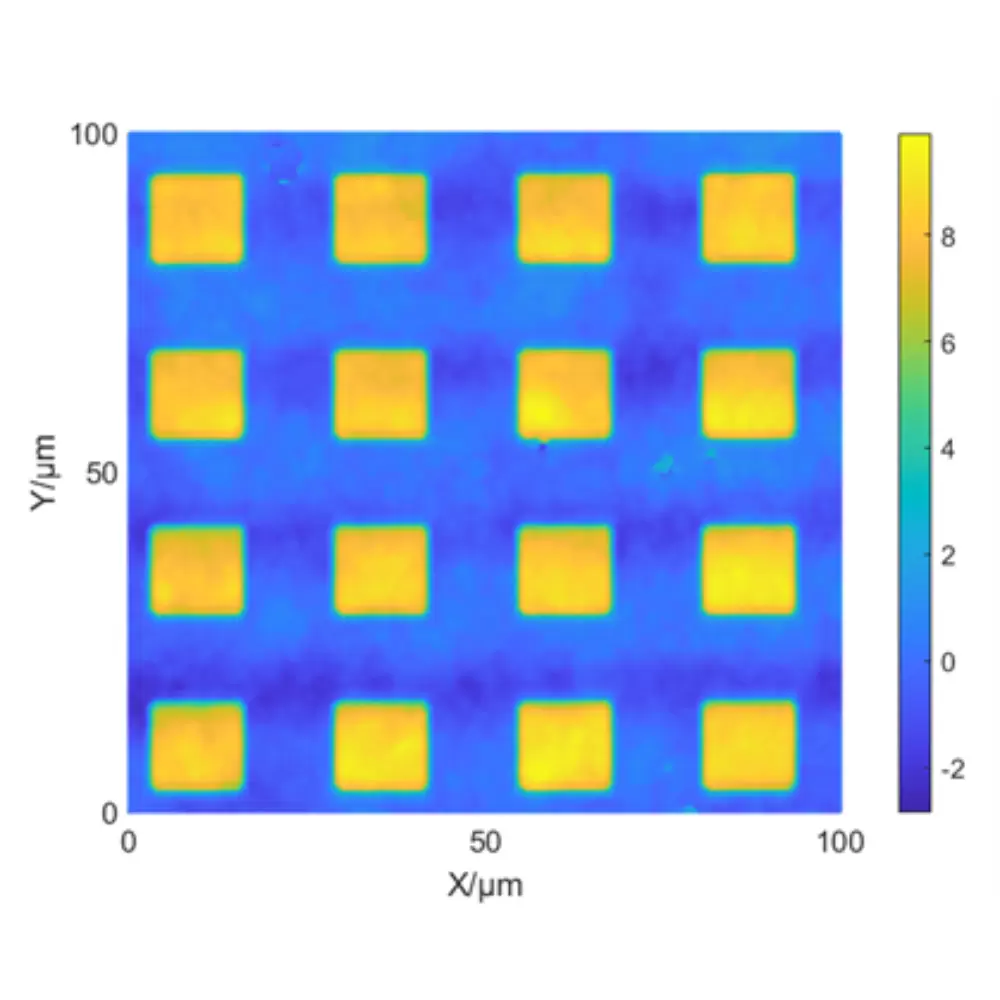 Girds Matrix
 -
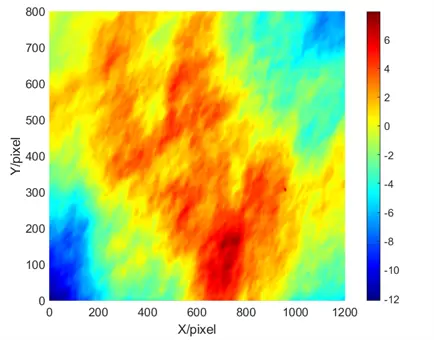 Polished Silicon Wafer


