Knowledge Center
Image Gallery


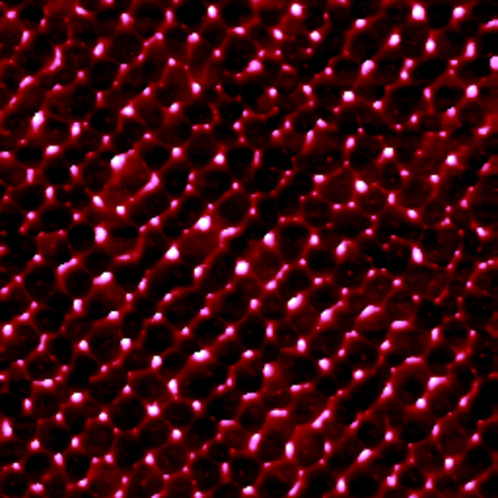
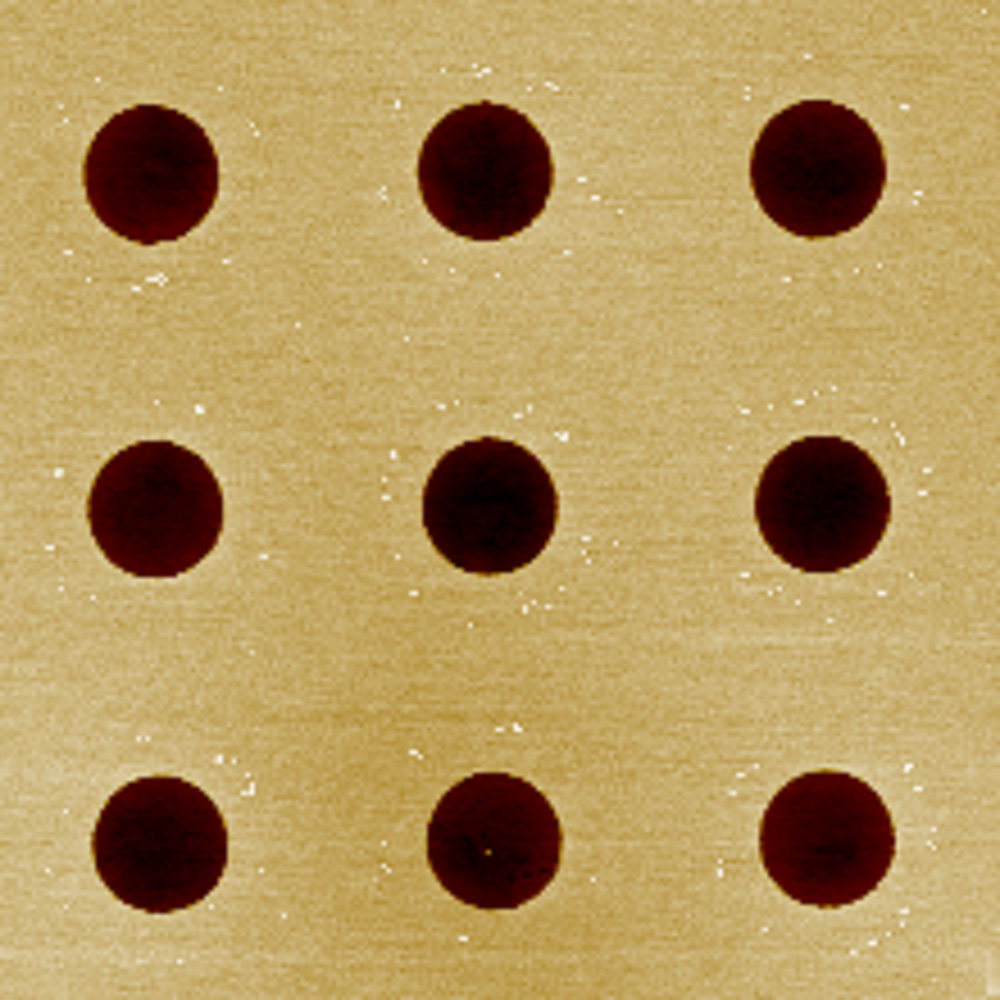
This is a micro-area scanning image of the electron transport layer (ETL) structure with a scanning range of 8 μm. By analyzing the size of the shadow part, it can provide a measurement basis for the improvement of the electron transport layer manufacturing process.
">