Filter by:
-
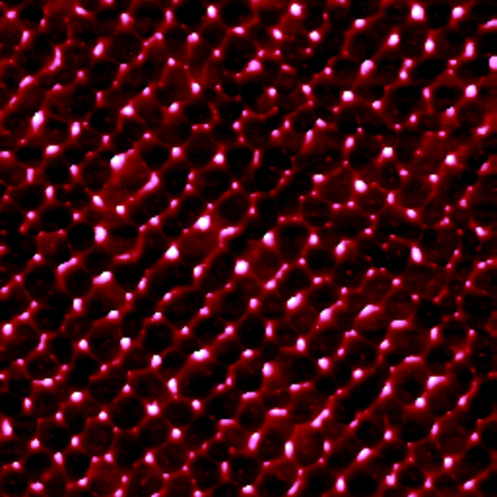
 LTPS Grain
 -
 PLZT
PLZT -
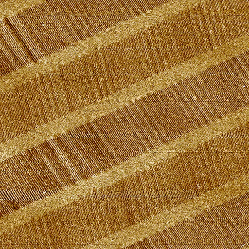 Tape Magnetic Domains
 -
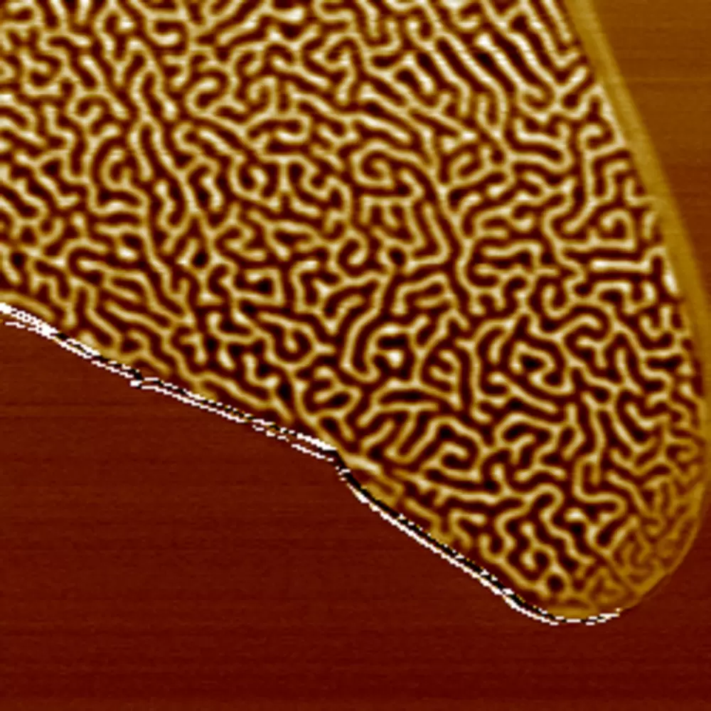
 LiNbO3 Ferroelectric Film
 -
 The Surface Potential of 2D Materials
 -
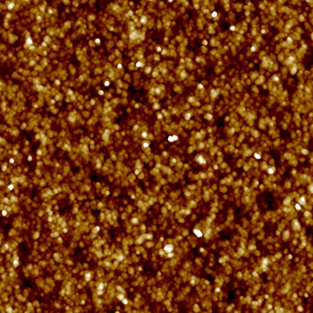
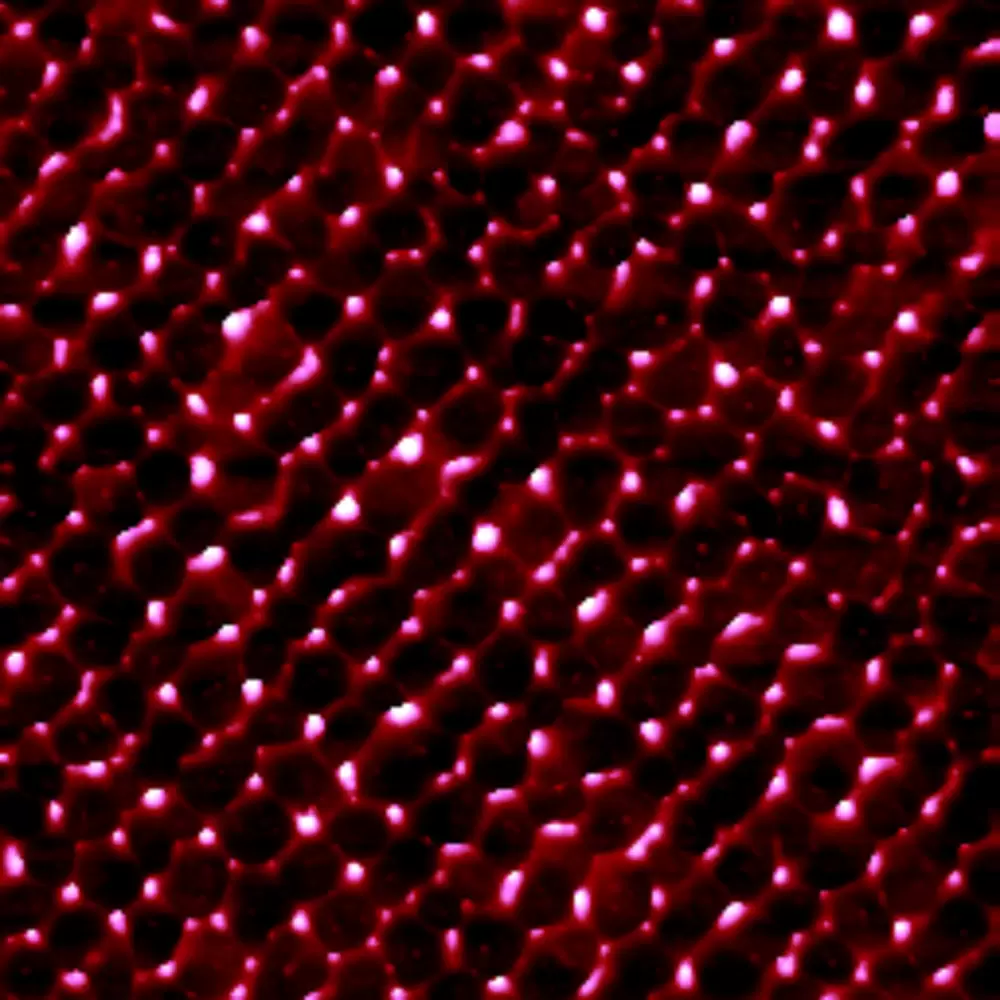
 2D Material's Magnetic Domains
 -
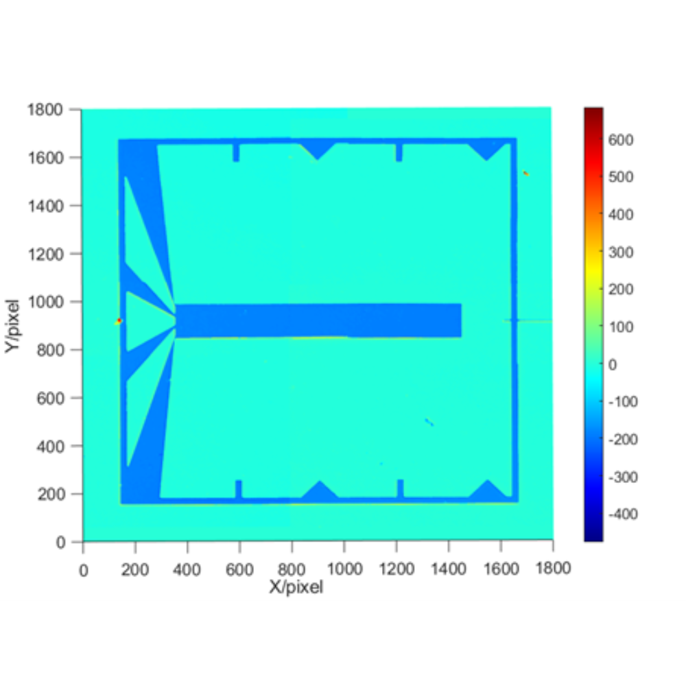
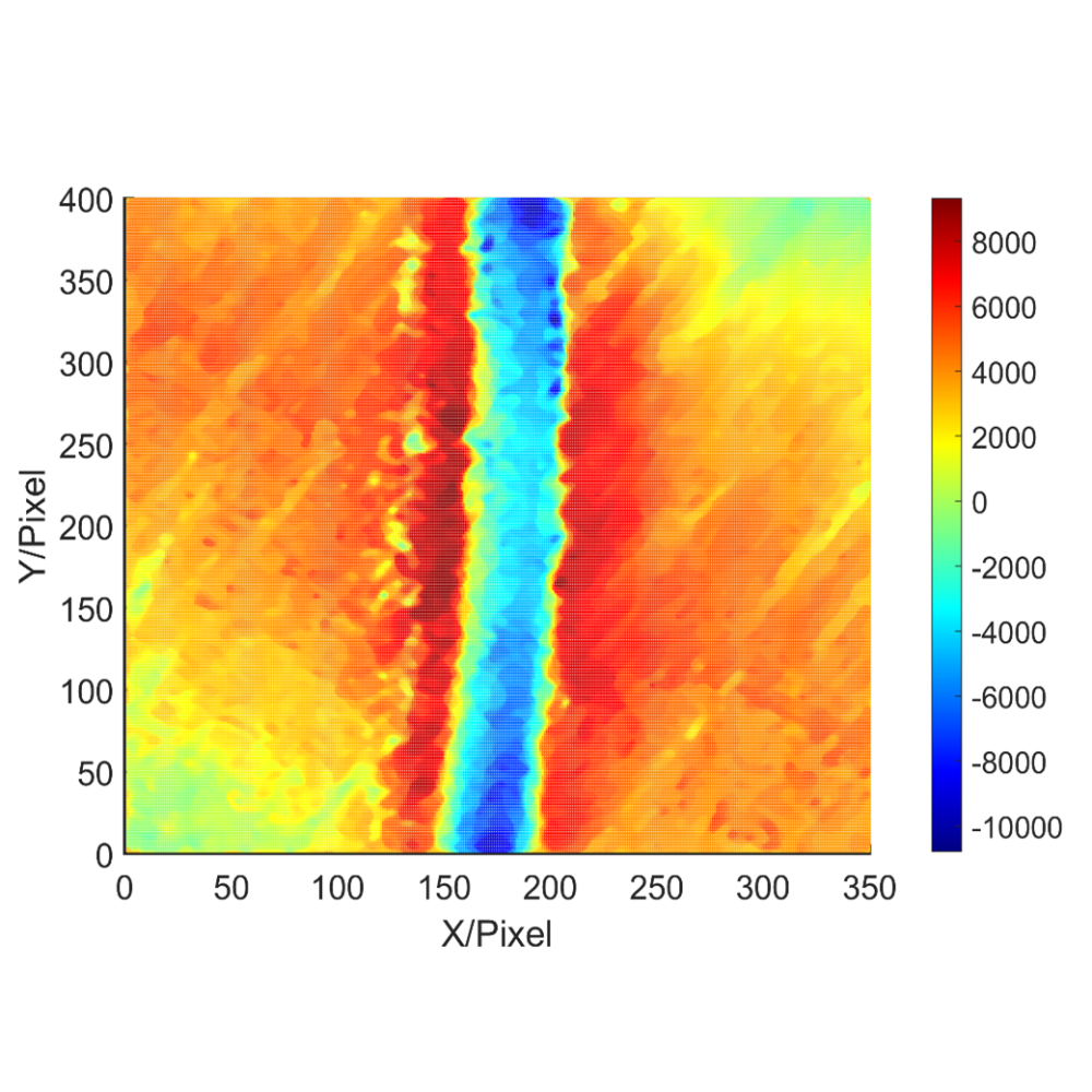
 Glass Substrate
 -
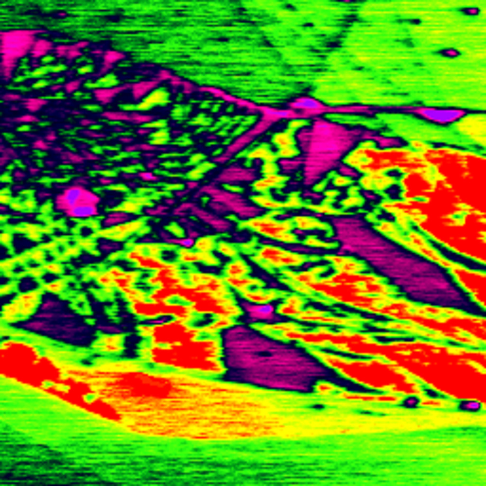
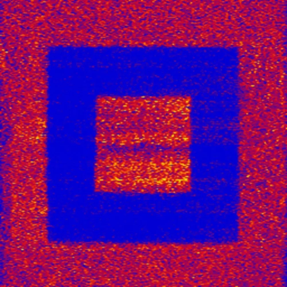 The Square-Shaped Pattern of the PZT Material
 -
 182 nm Standard Step Height
 -
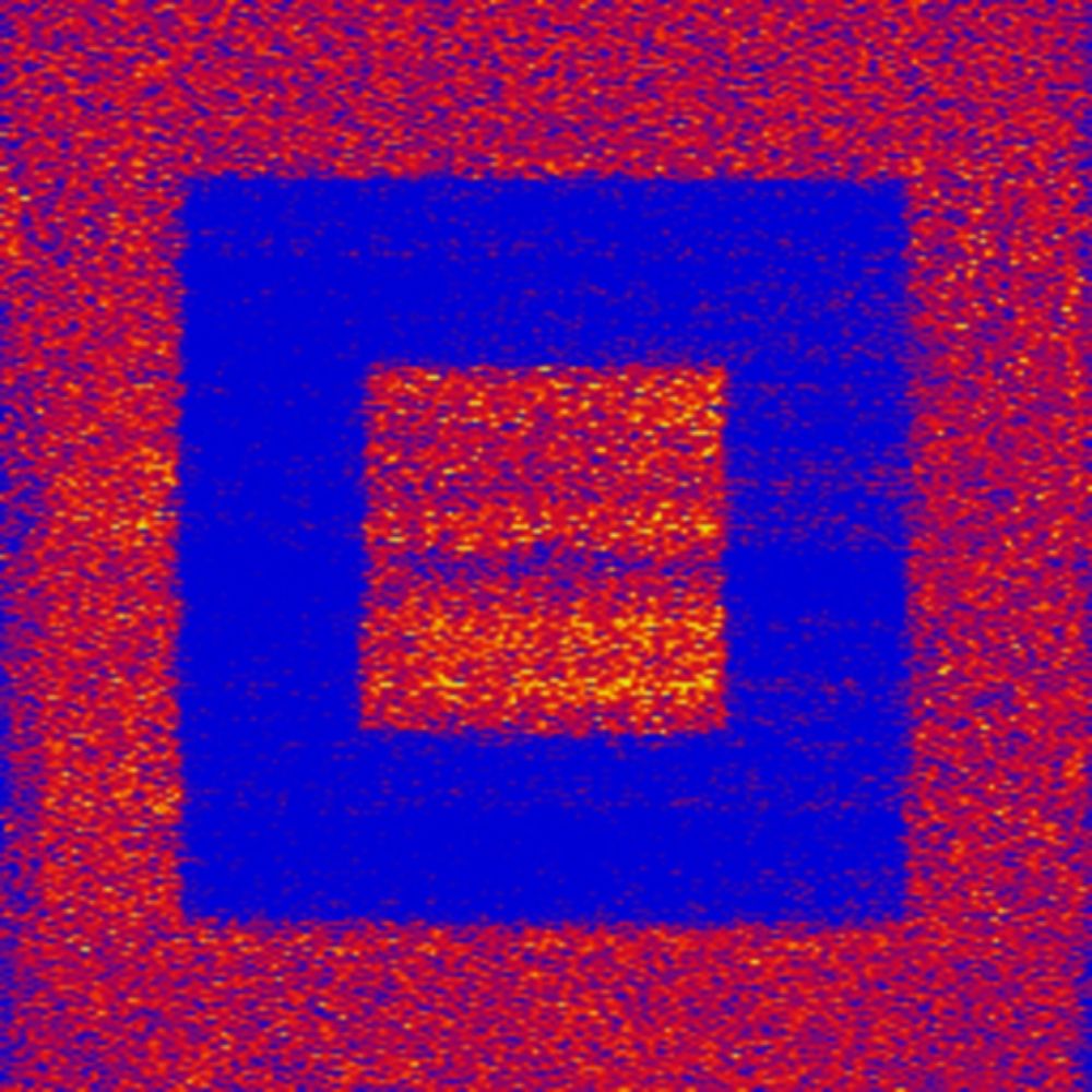
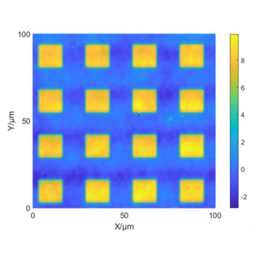
 Girds Matrix
 -
 Roughness Standard Sample
 -
 Laser Marked Sample
 -
 Lubricant Seal Cover
 -
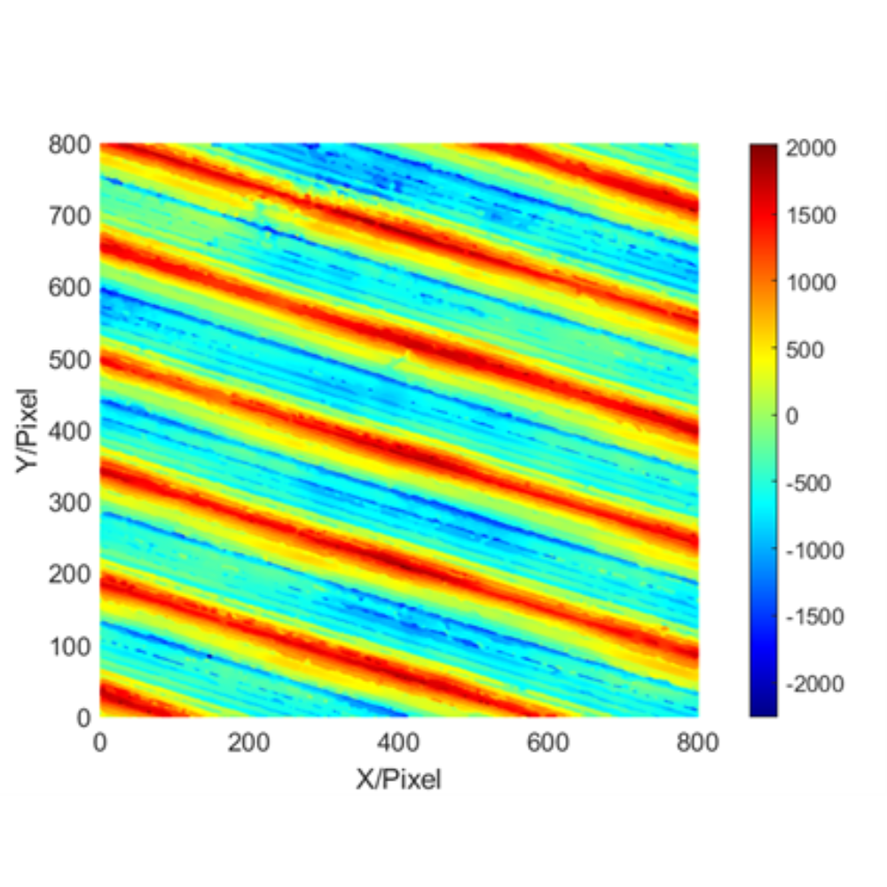
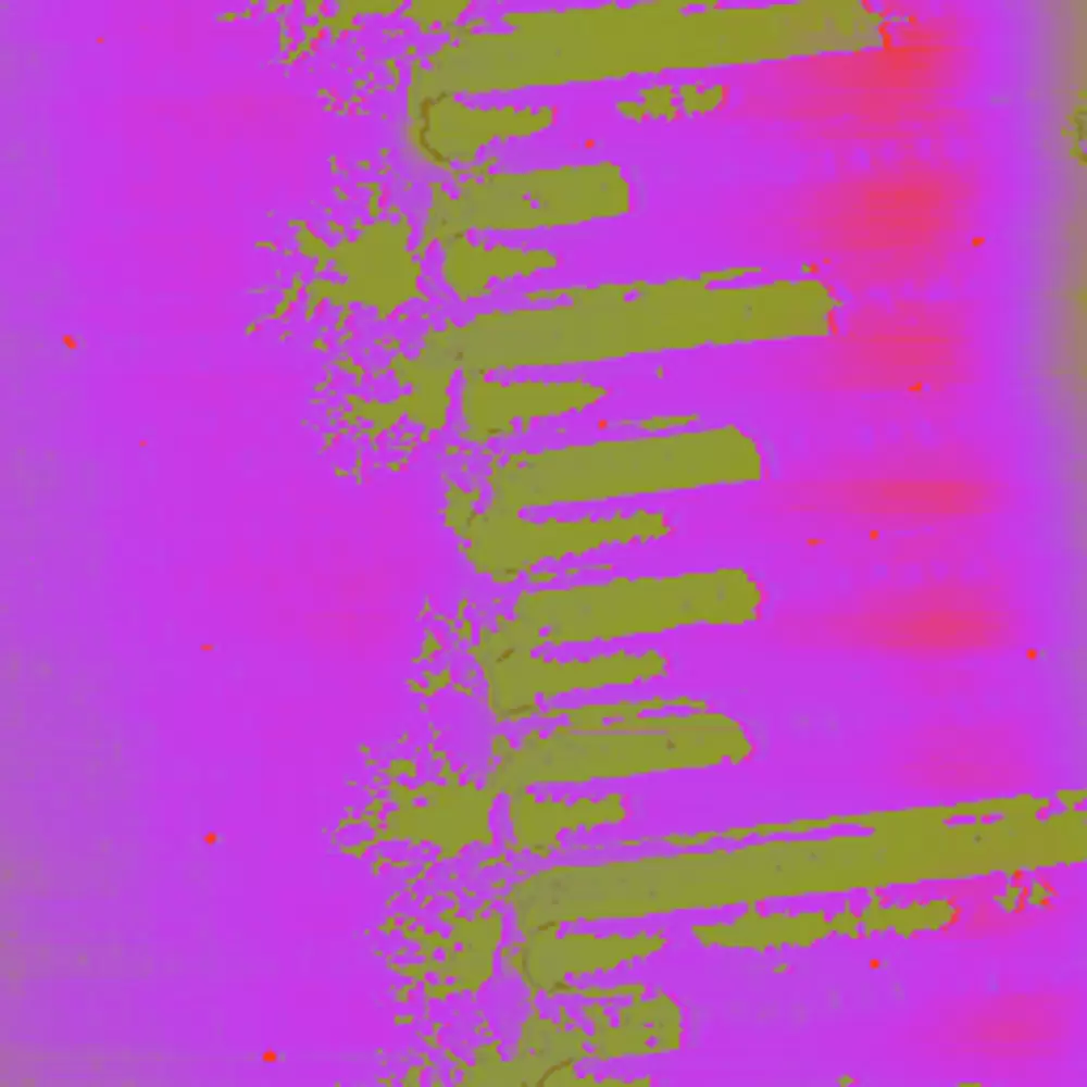
 Metal Groove
 -
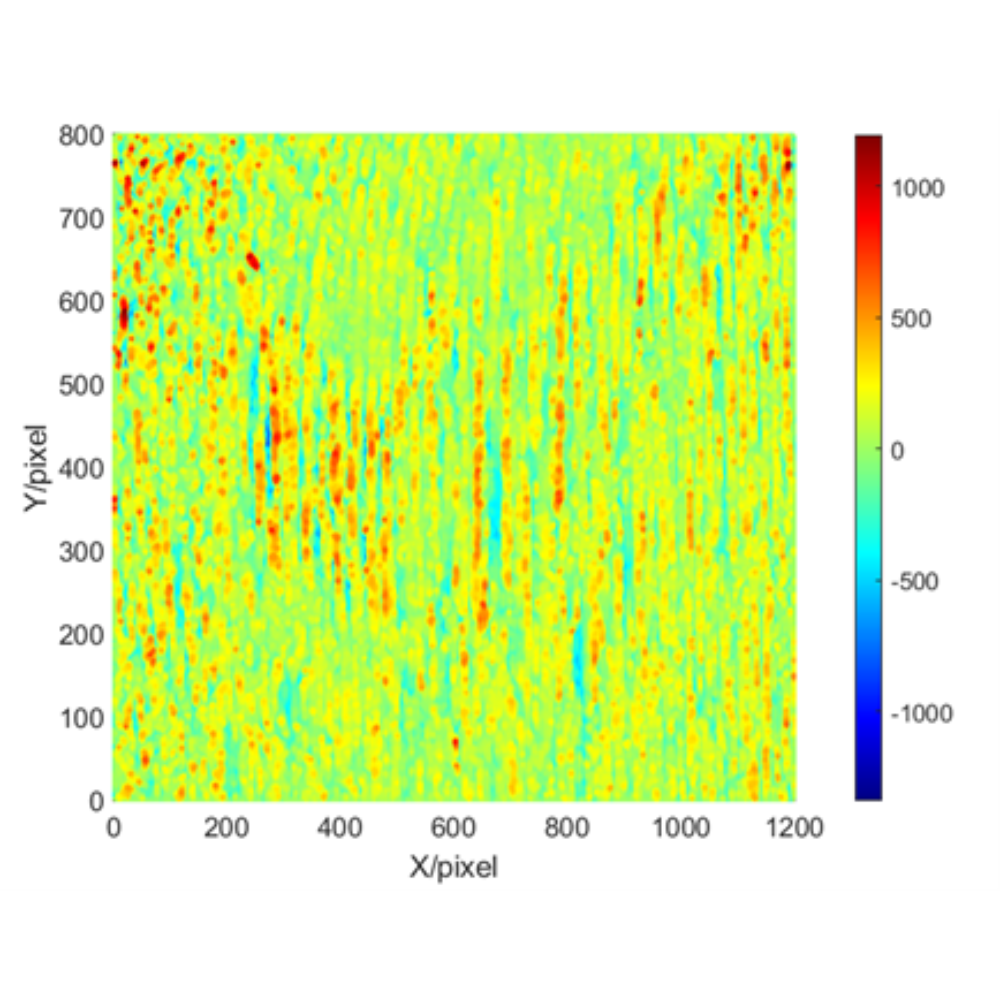
 Metal Scratch