Knowledge Center
Image Gallery


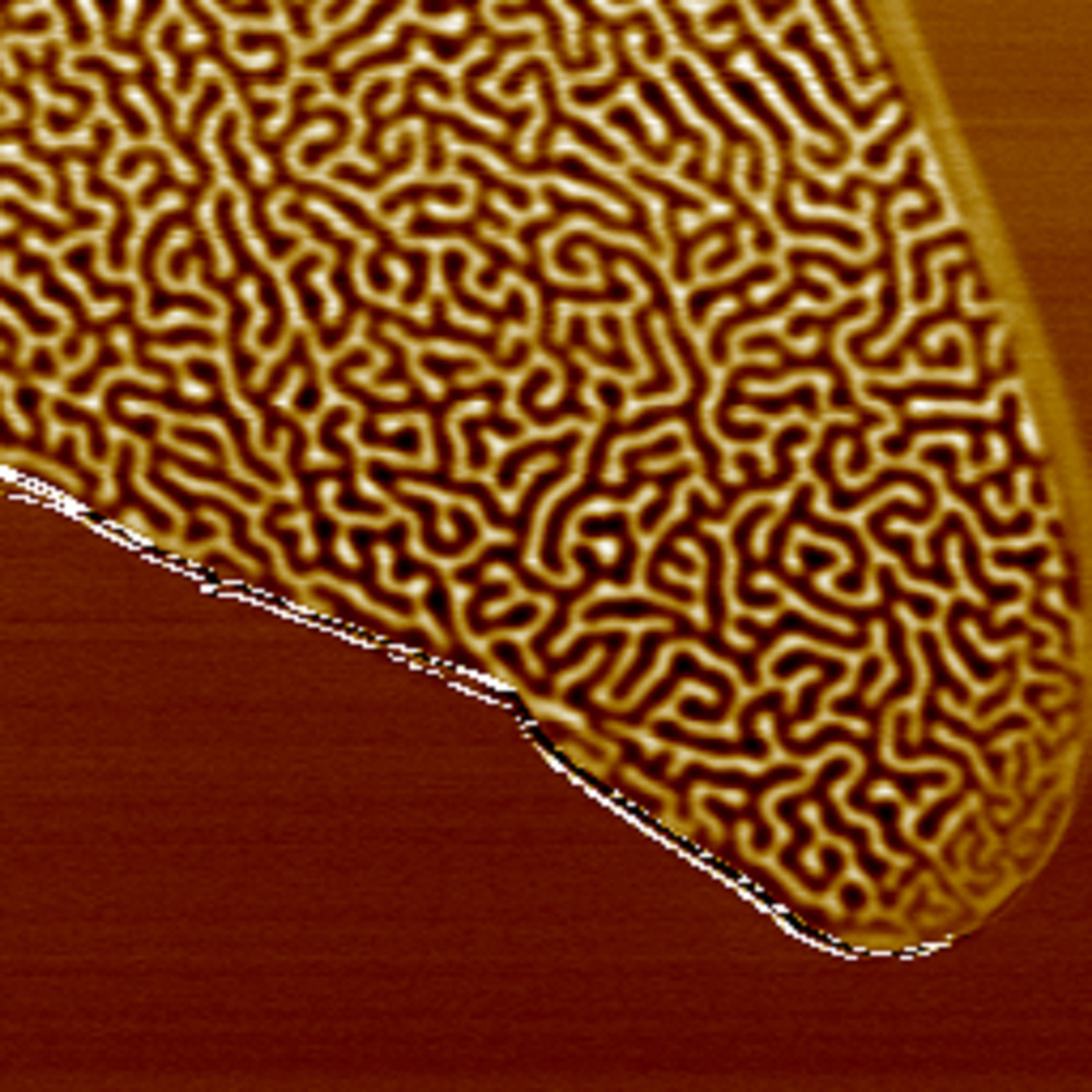 SiC Atomic Step
This is an image of SiC atomic step with a scanning range of 500 nm, and the step height is approximately 0.75 nm. SiC, as a representative material of wide bandgap semiconductors, is regarded as an ideal material for manufacturing high-power semiconductor devices.
">
Room 2109, 21st Floor, Building 2, Ruihong Enterprise World, 118 Feihong Road, Hongkou District, Shanghai
Copyright © 2025 FreeSpirit (Shanghai) Precision Instrument Co., Ltd Shanghai ICP No. 2025145947-1 Privacy Policy Sitemap


Copyright © 2025 FreeSpirit (Shanghai) Precision Instrument Co., Ltd Shanghai ICP No. 2025145947-1 Privacy Policy Sitemap