Precise Characterization of Atomic Force Microscope (AFM) Enables Microscopic Observation of Silicon Carbide (SiC) Surface Interfaces
SiC is a wide-bandgap semiconductor material. Due to its superior physical and electrical properties, it plays an increasingly vital role in the modern semiconductor industry, particularly in electronic devices operating under extreme conditions such as high voltage, high frequency, high temperature, and high power. Simultaneously, since parameters such as surface topography, crystal quality, and roughness significantly impact the performance of SiC materials and devices, AFM serves as an indispensable nanoscale surface analysis tool in SiC-related research and production.
Although SiC has outstanding electrical and thermal properties, numerous challenges persist in material preparation, crystal growth, surface treatment, and device fabrication—including surface roughness control, epitaxial layer quality, and crystal defects, etc. Therefore, to fully leverage exceptional performance of SiC, strict control over material quality, surface condition, and processing precision is essential. As a high-resolution, non-destructive surface measurement and analysis tool, AFM has become an indispensable instrument in SiC material and device R&D, production, and quality control. Through precise AFM characterization, researchers and engineers gain deep insights into the microscopic world of SiC surfaces and interfaces, continuously advancing SiC semiconductor technology toward higher performance and reliability.
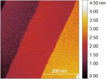
As shown in the figure below, this is the scanning result of FreeSpirit AFM. It shows a 500 nm scan range of SiC atomic steps, with a step height of approximately 0.75 nm.
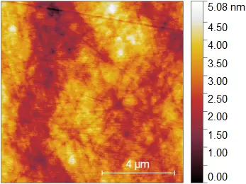
As shown in the figure below, this is an image obtained by scanning the SiC surface using a FreeSpirit AFM. The scanning range is 10 μm, and the roughness of the C-surface is 0.72 nm.
