The Key Role of Atomic Force Microscope (AFM) in LPTS Manufacturing and Quality Control
Low temperature polycrystalline silicon (LTPS) is a technology used to manufacture thin film transistors (TFT). It is widely applied in the modern display panel industry, particularly in high-end small-to-medium-sized display devices such as smartphones, tablet computers, automotive displays, premium laptops, and emerging flexible displays and AMOLED screens.
AFM plays an indispensable role in both the research and production testing of LTPS technology. This is mainly because the core of LTPS lies in the microscopic characteristics of its polycrystalline silicon thin film, including surface topography, grain structure, crystalline quality, and electrical property distribution. These characteristics directly affect the performance of TFT devices, such as mobility, threshold voltage, uniformity, and reliability. Uniform grain size enhances electron mobility; surface roughness affects the uniformity and interface quality of subsequent processes such as gate insulation layer and source/drain formation; defective grain boundaries impair carrier transport and device consistency; crystalline defects and voids reduce the electrical stability and lifetime of TFT.
As an ultra-high-resolution, non-destructive tool for analyzing surface topography and material properties, AFM enables nanoscale or even atomic-level characterization of nanoscale features such as surface roughness, grain size and distribution, grain boundary density and orientation, crystalline defects, and voids. It provides key data support for process optimization, defect analysis, mechanism research, and yield improvement in the modern display panel industry, particularly for LTPS applications.
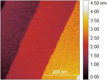
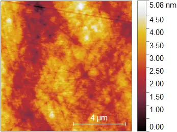
The following two AFM scan images of LTPS demonstrate the measurement capabilities of the FreeSpirit AFM. The two images below show LTPS grains with slightly different crystal orientations, both scanned over a 5 μm area. Both images show a roughness of approximately 10 nm, uniform grain distribution without obvious defects, and grain sizes around 150 nm.
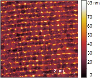
LTPS Surface Crystalline Grain Orientation Image
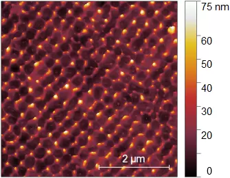
LTPS Surface Crystalline Grain Orientation Image


