Unveil the Powerful Applications of Atomic Force Microscope (AFM) in 2D Materials from the Surface Morphology to Surface Potential of h-BN
As one of the major breakthroughs in 21st-century materials science, 2D materials demonstrate revolutionary application potential across electronics, energy, sensing, optoelectronics, medicine, and environmental fields due to their unique structures and exceptional properties. Despite facing challenges in preparation, stability, integration, and other aspects, with the continuous advancement of technology and in-depth research, 2D materials are expected to drive technological innovation in multiple industries in the coming decades, becoming the core foundational material for building the next generation of intelligent, flexible, and efficient devices.
Graphene, transition metal dichalcogenides (e.g., MoS₂), black phosphorus (BP), hexagonal boron nitride (h-BN), MXene, and 2D transition metal carbides/nitrides are all representative examples of 2D materials. With its high spatial resolution, multimodal measurement capabilities, low sample damage, and adaptability across diverse environments, AFM plays a central role in fundamental research, performance characterization, and device application exploration of 2D materials. It remains one of the most critical characterization tools, particularly for thickness measurement, surface topography, nanomechanical and nanoelectrical property analysis, and heterostructure investigation.
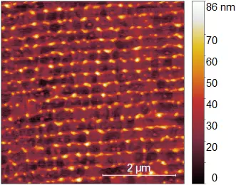
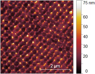
The following shows typical results obtained using the FreeSpirit AFM to test 2D materials, with h-BN serving as an example. As shown in the following figures, these are topographical and surface potential images of hexagonal boron nitride (h-BN) with a scanning range of 10 μm. Analysis of the topographical image reveals that the thickness of this h-BN monolayer is approximately 0.3 nm, with a surface roughness of about 0.4 nm in the flat regions. The surface potential image clearly shows the irregular distribution of surface potential within the specially treated h-BN. Analysis of h-BN thickness, surface roughness, and surface potential provides intuitive data support for understanding the effects of layer number on electronic and lattice structures, as well as local work function variations induced by doping effects.
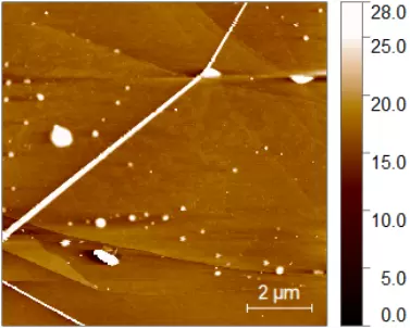
h-BN Surface Topography Image (Vertical Coordinates Unit: nm)
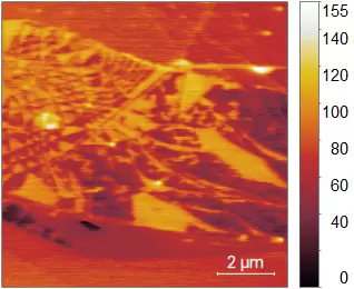
h-BN Surface Potential Image (Vertical Coordinates Unit: mV)


