Home
Home
Products
Products
Atomic Force Microscope (AFM)
AFM-Baritone
AFM-Piccolo
AFM-Tuba
AFM-Tenor
AFM-Tuner
White Light Interferometry (WLI)
WLI-Marimba
Integrated Systems
AFM-WLI Duet
Accessories
AFM Probes
Applications
Applications
Semiconductor
Display
2D Materials
Thin Film
Knowledge Center
Knowledge Center
Image Gallery
Case Studies
Webinars
FreeSpirit Academy
Download Center
News & Events
News & Events
News
Events
Company
Company
Overview
Careers
Social Media
Contact
Contact
Contact Information
Online Enquiries
EN
EN
中
×
Knowledge Center
Image Gallery
Current Location:
Home
>
Knowledge Center
>
Image Gallery
Filter by:
System
All
AFM-Piccolo
AFM-Baritone
AFM-Tenor
AFM-Tuba
AFM-Tuner
WLI-Marimba
AFM-WLI Duet
Application
All
Semiconductor
Display
2D Materials
Thin films
Polymer
MEMS
Metals
Optical Element
Metal
System
All
AFM-Piccolo
AFM-Baritone
AFM-Tenor
AFM-Tuba
AFM-Tuner
WLI-Marimba
AFM-WLI Duet
Application
All
Semiconductor
Display
2D Materials
Thin films
Polymer
MEMS
Metals
Optical Element
Metal
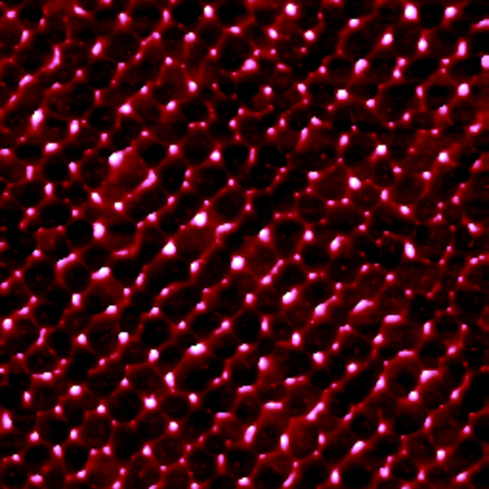
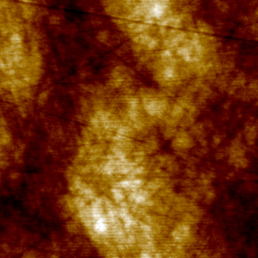
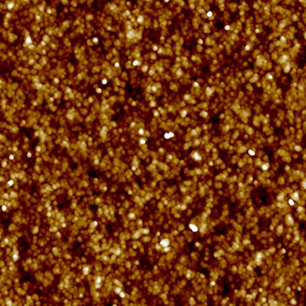
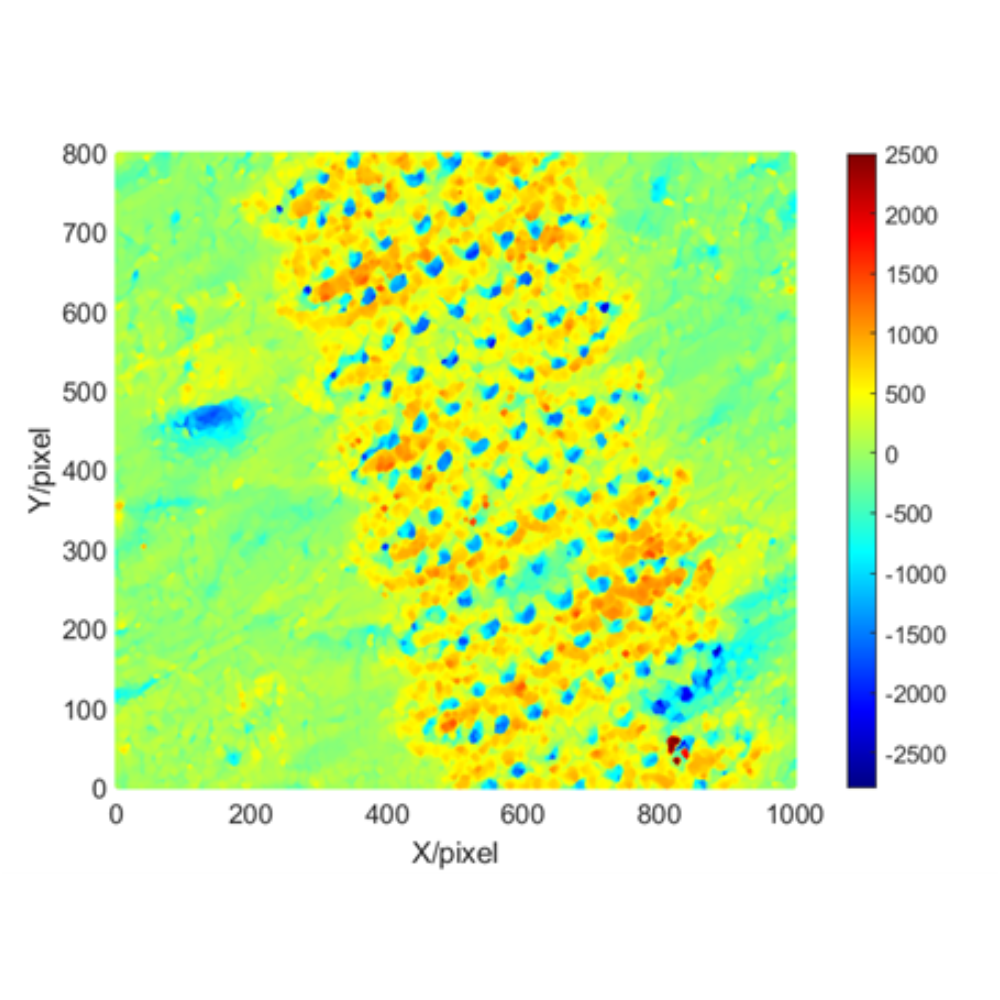
LTPS Grain
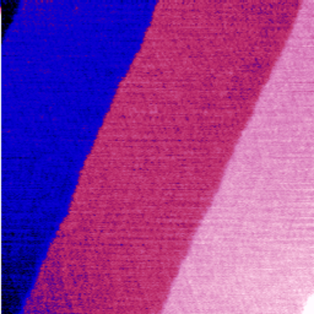
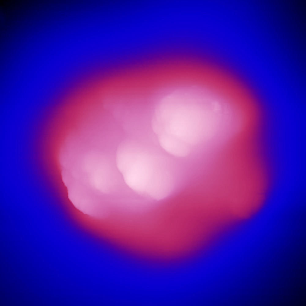
The Surface Potential of Au-Al Material
SiC Atomic Step
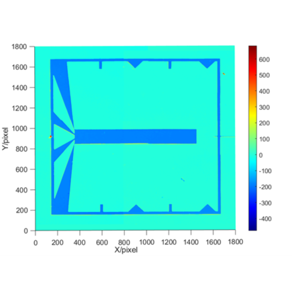
Patterned Sapphire Substrate (PSS)
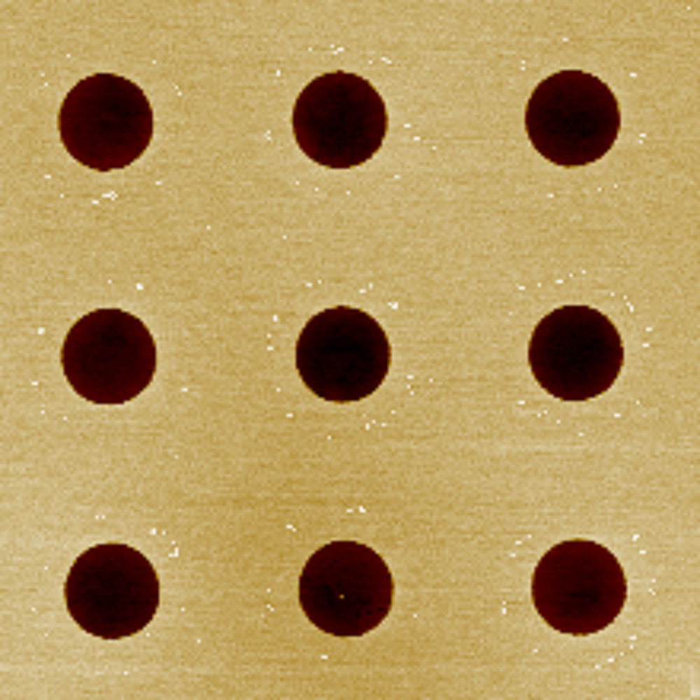
CMP Micro-Holes Array
OLED Pattern
ETL Structure
SiC Surface
The Edge Structure of PSS
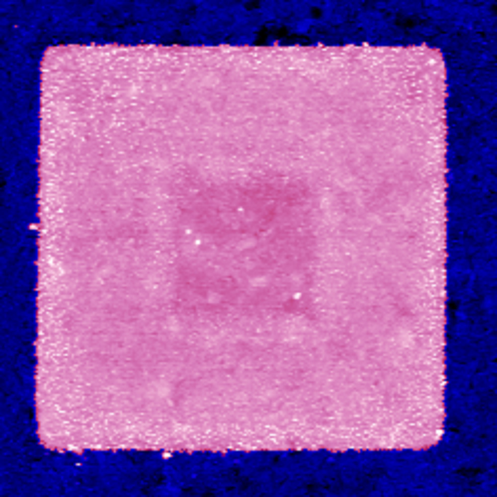
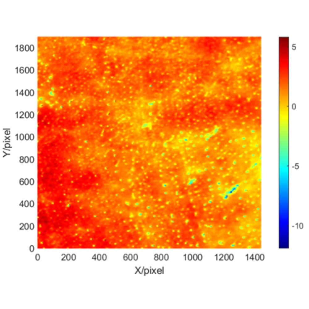
The Surface Potential of SRAM
Standard Wafer
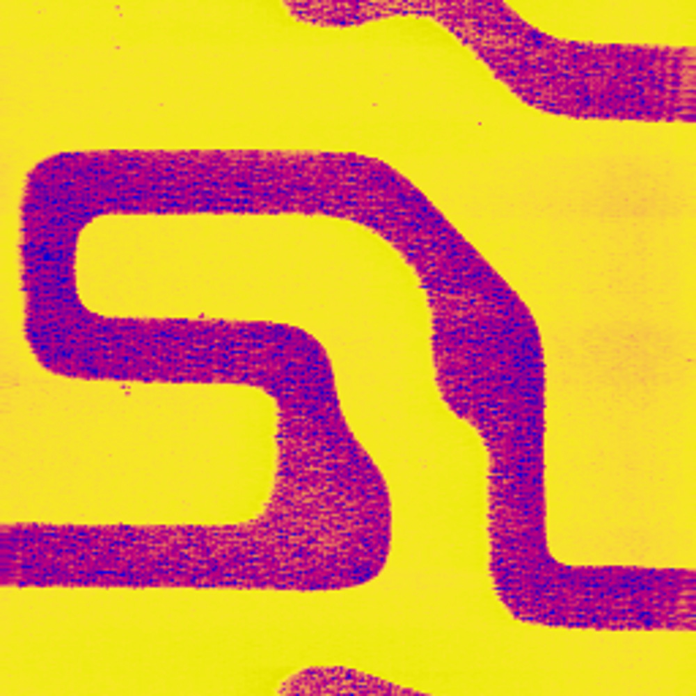
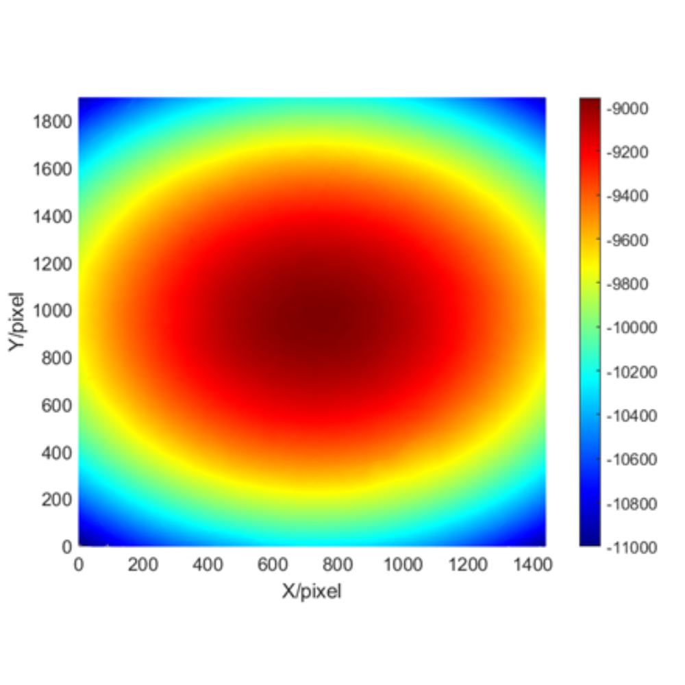
Microelectrode
Polymer Particle
Glass Substrate
Flat Mirror
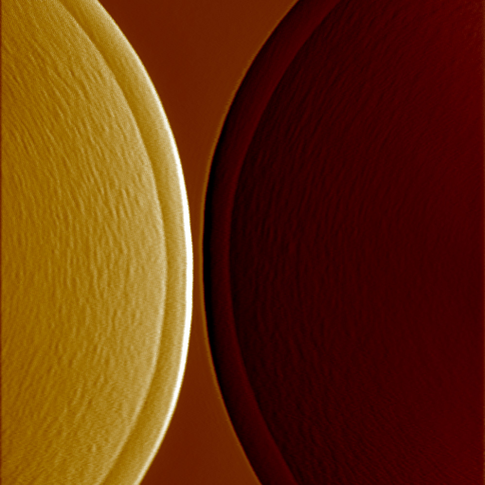
Convex Lens
182 nm Standard Step Height
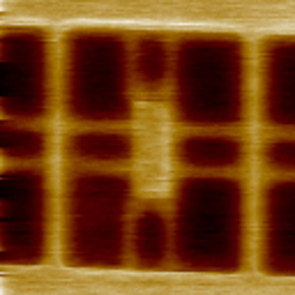
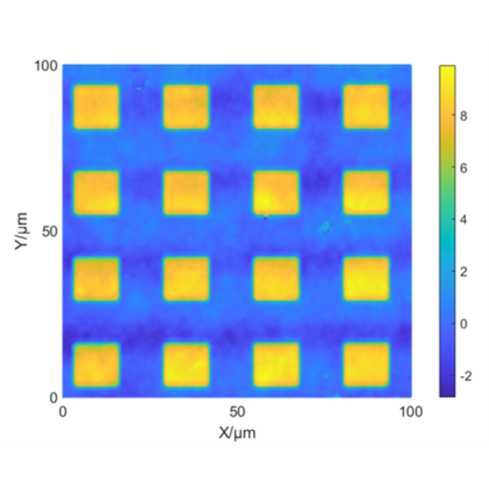
Girds Matrix
Roughness Standard Sample
Laser Marked Sample
|<
<
1
2
>
>|
Contact
Top
FreeSpirit (Shanghai) Precision Instrument Co., Ltd
EN
中
Home
Products
Atomic Force Microscope (AFM)
White Light Interferometry (WLI)
Integrated Systems
Accessories
Applications
Semiconductor
Display
2D Materials
Thin Film
Knowledge Center
Image Gallery
Case Studies
Webinars
FreeSpirit Academy
Download Center
News & Events
News
Events
Company
Overview
Careers
Social Media
Contact
Contact Information
Online Enquiries