Atomic Force Microscopy (AFM): A Key Enabler from Semiconductor Fundamental Research to Industrial Applications
As a powerful tool for nanoscale characterization, AFM plays a key role in the semiconductor field, spanning fundamental research to industrial applications. It not only provides critical data support for semiconductor device design, manufacturing, and optimization but also offers irreplaceable advantages in driving the continued development of Moore's Law and the application of novel semiconductor materials (such as wide-bandgap semiconductors and 2D materials).
As semiconductor technology advances toward higher integration, smaller dimensions, and greater functionality, AFM technology itself continues to evolve (e.g., high-speed AFM, multi-mode combined AFM). Its applications in the field of the semiconductor industry will become increasingly widespread and profound in the future.
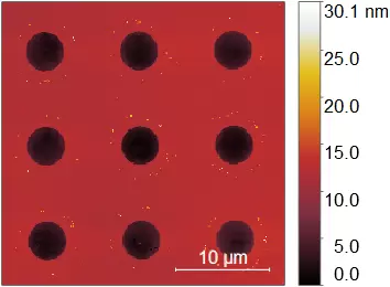
As shown in the following figure, this is a micropore array image processed by CMP with 30 μm scan range. CMP is a key process for wafer planarization. Measuring surface roughness and topography provides robust assurance for improving the CMP process.
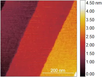
As shown in the following figure, this is a SiC atomic-scale step image with 500 nm scan range, and the step height is approximately 0.75 nm. As a representative wide-bandgap semiconductor material, SiC is considered an ideal candidate for high-power semiconductor devices.
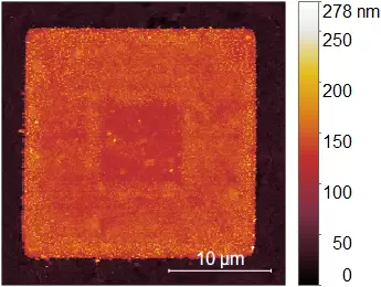
As shown in the following figure, this is a microelectrode surface topography image with 28 μm scan range, and its height is approximately 120 nm. The detection of microelectrode surface roughness and height provides robust assurance for the improvement of its manufacturing and processing techniques.
