The Role of Atomic Force Microscopy (AFM) in LTPS Technology Research and Production Testing
Low temperature polycrystalline silicon (LTPS) is a technology used to manufacture thin film transistors (TFT). It is widely applied in the modern display panel industry, particularly in high-end small-to-medium-sized display devices such as smartphones, tablet computers, automotive displays, premium laptops, and emerging flexible displays and AMOLED (Active-Matrix Organic Light-Emitting Diode) screens.
AFM plays an indispensable role in both research and production testing for LTPS technology. This is mainly because the core of LTPS lies in the microscopic characteristics of its polycrystalline silicon thin film, including surface topography, crystalline quality, grain structure, and electrical property distribution. These characteristics directly affect the performance of TFT devices, such as mobility, threshold voltage, uniformity, and reliability. As an ultra-high-resolution, non-destructive tool for surface topography and material property analysis, AFM enables nanoscale or even atomic-level characterization of the nanoscale features. It provides key data support for LTPS process optimization, defect analysis, mechanism research, and yield improvement.
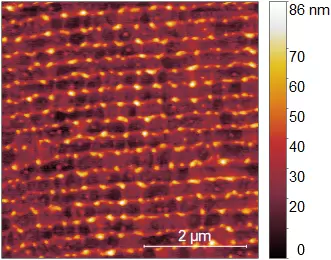
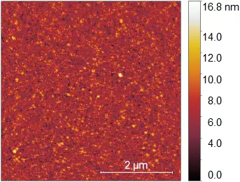
As shown in the following figure, this is an LTPS grain image with 5 μm scan range. The surface roughness is approximately 10 nm, and the grain size is about 150 nm.

As a key basic material for transparent conductivity, ITO glass plays a crucial role in display technologies such as liquid crystal displays, OLEDs, and touchscreens. Its performance directly impacts display quality, touch sensitivity, and device lifespan.
AFM provides high-resolution, multidimensional analysis of ITO film surface and electrical properties, offering unparalleled advantages in surface topography, roughness, thickness, conductive uniformity, and microscopic defects. It serves as a key characterization tool throughout R&D, production, and failure analysis processes.
The synergy between high-performance ITO materials and precision AFM characterization technology jointly propels panel display technology toward higher resolution, thinner profiles, enhanced flexibility, and greater sensitivity.
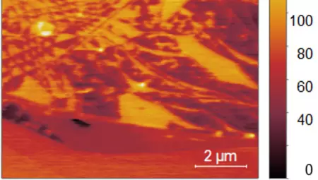
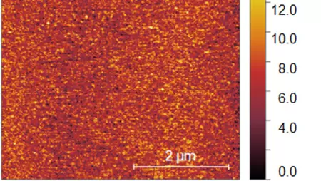
As shown in the following figure, this is an OLED surface image with 5 μm scan range, and the surface roughness is 1.27 nm.


