The Essential Role of Atomic Force Microscopy (AFM) in Thin Film Research
As one of the basic materials in modern technology, nanoscale thin films play a key role in multiple cutting-edge fields, such as electronics, energy, biology, and optics. Precise characterization and performance regulation of these films are crucial for achieving functionalization and high performance.
AFM with its ultra-high resolution, rich characterization dimensions, and non-destructive nature, has become one of the most important and commonly used tools in nanoscale film research. It not only provides the high resolution images of film surface topography and the information on step heights and roughness, but also enables in-depth analysis of mechanical, electrical, and tribological properties, offering robust technical support for the design, optimization, and application of thin-film materials. Consequently, AFM holds an irreplaceable position in the field of nanoscale thin film measurement and characterization, serving as a key technology driving progress in nanotechnology and nano manufacturing.
The following are some results of thin films tested by FreeSpirit AFM:
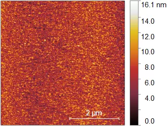
As shown in the following figure, this is an ITO thin film surface topography image with 5 μm scan range, and the surface roughness is 1.46 nm.

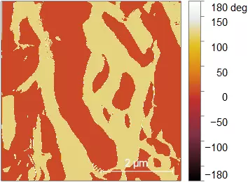
As shown in the following figure, this is a PLZT thin film Lockin Phase image with 5 μm scan range. The red and yellow regions represent different piezoelectric domains with a phase difference of 180°.


