Knowledge Center
Technical Notes


2D materials refer to novel nanomaterials with thicknesses of a single atom or a few atomic layers. Their most representative example is graphene, which also includes transition metal dichalcogenides (e.g., MoS₂), black phosphorus (BP), hexagonal boron nitride (h-BN), MXene, and 2D transition metal carbides/nitrides. These materials exhibit broad application prospects across multiple fields due to their unique physical, chemical, and electronic properties.
As one of the major breakthroughs in 21st-century materials science, 2D materials demonstrate revolutionary application potential across electronics, energy, sensing, optoelectronics, medicine, and environmental fields due to their unique structures and exceptional properties. Despite facing challenges in preparation, stability, integration, and other aspects, with the continuous advancement of technology and in-depth research, 2D materials are expected to drive technological innovation in multiple industries in the coming decades, becoming the core foundational material for building the next generation of intelligent, flexible, and efficient devices.
The following are some results of 2D materials tested by FreeSpirit AFM:
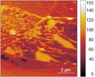
As shown in the following figure, this is a hexagonal boron nitride (h-BN) surface potential image with 10 μm scan range. The image clearly reveals the irregular distribution of surface potential within the h-BN structure.
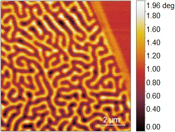
As shown in the following figure, this is an image of the magnetic domain distribution in a certain 2D material with 10 μm scan range. The "maze-like" distribution of magnetic domains inside the material can be clearly seen in the image.

留言提交中... |